ZHCSE70D August 2015 – September 2017 TMDS181
PRODUCTION DATA.
- 1 特性
- 2 应用
- 3 说明
- 4 修订历史记录
- 5 Pin Configuration and Functions
-
6 Specifications
- 6.1 Absolute Maximum Ratings
- 6.2 ESD Ratings
- 6.3 Recommended Operating Conditions
- 6.4 Thermal Information
- 6.5 Power Supply Electrical Characteristics
- 6.6 TMDS Differential Input Electrical Characteristics
- 6.7 TMDS Differential Output Electrical Characteristics
- 6.8 DDC, I2C, HPD, and ARC Electrical Characteristics
- 6.9 Power-Up and Operation Timing Requirements
- 6.10 TMDS Switching Characteristics
- 6.11 HPD Switching Characteristics
- 6.12 DDC and I2C Switching Characteristics
- 6.13 Typical Characteristics
- 7 Parameter Measurement Information
-
8 Detailed Description
- 8.1 Overview
- 8.2 Functional Block Diagram
- 8.3
Feature Description
- 8.3.1 Reset Implementation
- 8.3.2 Operation Timing
- 8.3.3 Swap and Polarity Working
- 8.3.4 TMDS Inputs
- 8.3.5 TMDS Inputs Debug Tools
- 8.3.6 Receiver Equalizer
- 8.3.7 Input Signal Detect Block
- 8.3.8 Audio Return Channel
- 8.3.9 Transmitter Impedance Control
- 8.3.10 TMDS Outputs
- 8.3.11 Pre-Emphasis/De-Emphasis
- 8.4 Device Functional Modes
- 8.5 Register Maps
- 9 Application and Implementation
- 10Power Supply Recommendations
- 11Layout
- 12器件和文档支持
- 13机械、封装和可订购信息
11 Layout
11.1 Layout Guidelines
For the TMDS181 on a high-K board: It is required to solder the PowerPAD™ onto the thermal land to ground. A thermal land is the area of solder-tinned-copper underneath the PowerPAD package. On a high-K board, the TMDS181 can operate over the full temperature range by soldering the PowerPAD onto the thermal land.
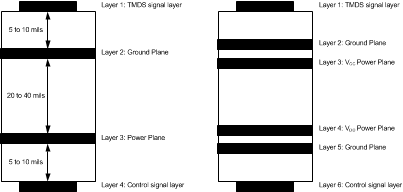
On a low-K board: For the device to operate across the temperature range on a low-K board, the designer must use a 1-oz Cu trace connecting the GND pins to the thermal land. A simulation shows RθJA = 100.84°C/W allowing 545 mW power dissipation at 70°C ambient temperature. A general PCB design guide for PowerPAD packages is provided in PowerPAD Thermally Enhanced Package, SLMA002. TI recommends using at a minimum a four-layer stack to accomplish a low-EMI PCB design. TI recommends six layers as the TMDS181 is a two-voltage-rail device.
- Routing the high-speed TMDS traces on the top layer avoids the use of vias (and their discontinuities) and allows for clean interconnects from the HDMI connectors to the retimer inputs and outputs. It is important to match the electrical length of these high-speed traces to minimize both inter-pair and intra-pair skew.
- Placing a solid ground plane next to the high-speed single layer establishes controlled impedance for transmission link interconnects and provides an excellent low-inductance path for the return current flow.
- Placing a power plane next to the ground plane creates an additional high-frequency bypass capacitance.
- Routing slower-speed control signals on the bottom layer allows for greater flexibility because these signal links usually have margin to tolerate discontinuities such as vias.
- If an additional supply voltage plane or signal layer is needed, add a second power/ground plane system to the stack to keep symmetry. This makes the stack mechanically stable and prevents it from warping. Also, the power and ground plane of each power system can be placed closer together, thus increasing the high-frequency bypass capacitance significantly.
 Figure 38. Recommended 4- or 6-Layer PCB Stack
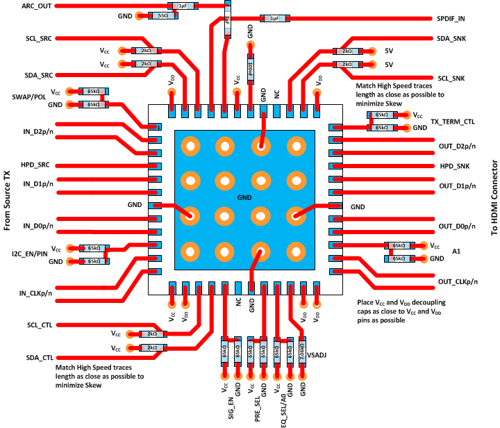
11.2 Layout Example
