ZHCSIX4I August   2007  – June 2024 TMP102

PRODUCTION DATA  

  1.   1
  2. 特性
  3. 应用
  4. 说明
  5. Pin Configuration and Functions
  6. Specifications
    1. 5.1 Absolute Maximum Ratings
    2. 5.2 ESD Ratings
    3. 5.3 Recommended Operating Conditions
    4. 5.4 Thermal Information
    5. 5.5 Electrical Characteristics
    6. 5.6 Timing Requirements
    7. 5.7 Typical Characteristics
  7. Detailed Description
    1. 6.1 Overview
    2. 6.2 Functional Block Diagram
    3. 6.3 Feature Description
      1. 6.3.1  Digital Temperature Output
      2. 6.3.2  Serial Interface
      3. 6.3.3  Bus Overview
      4. 6.3.4  Serial Bus Address
      5. 6.3.5  Writing and Reading Operation
      6. 6.3.6  Target Mode Operations
        1. 6.3.6.1 Target Receiver Mode
        2. 6.3.6.2 Target Transmitter Mode
      7. 6.3.7  SMBus Alert Function
      8. 6.3.8  General Call
      9. 6.3.9  High-Speed (HS) Mode
      10. 6.3.10 Timeout Function
      11. 6.3.11 Timing Diagrams
    4. 6.4 Device Functional Modes
      1. 6.4.1 Continuous-Conversion Mode
      2. 6.4.2 Extended Mode (EM)
      3. 6.4.3 Shutdown Mode (SD)
      4. 6.4.4 One-Shot/Conversion Ready (OS)
      5. 6.4.5 Thermostat Mode (TM)
        1. 6.4.5.1 Comparator Mode (TM = 0)
        2. 6.4.5.2 Interrupt Mode (TM = 1)
    5. 6.5 Programming
      1. 6.5.1 Pointer Register
      2. 6.5.2 Temperature Register
      3. 6.5.3 Configuration Register
        1. 6.5.3.1 Shutdown Mode (SD)
        2. 6.5.3.2 Thermostat Mode (TM)
        3. 6.5.3.3 Polarity (POL)
        4. 6.5.3.4 Fault Queue (F1/F0)
        5. 6.5.3.5 Converter Resolution (R1/R0)
        6. 6.5.3.6 One-Shot (OS)
        7. 6.5.3.7 EM Bit
        8. 6.5.3.8 Alert (AL Bit)
        9. 6.5.3.9 Conversion Rate (CR)
      4. 6.5.4 High- and Low-Limit Registers
  8. Application and Implementation
    1. 7.1 Application Information
    2. 7.2 Typical Application
      1. 7.2.1 Design Requirements
      2. 7.2.2 Detailed Design Procedure
      3. 7.2.3 Application Curve
    3. 7.3 Power Supply Recommendations
    4. 7.4 Layout
      1. 7.4.1 Layout Guidelines
      2. 7.4.2 Layout Example
  9. Device and Documentation Support
    1. 8.1 Documentation Support
      1. 8.1.1 Related Documentation
    2. 8.2 接收文档更新通知
    3. 8.3 支持资源
    4. 8.4 Trademarks
    5. 8.5 静电放电警告
    6. 8.6 术语表
  10. Revision History
  11. 10Mechanical, Packaging, and Orderable Information

封装选项

机械数据 (封装 | 引脚)
散热焊盘机械数据 (封装 | 引脚)
订购信息

Application Curve

Figure 7-3 shows the step response of the TMP102 device to a submersion in an oil bath of 100°C from room temperature (27°C). The time-constant, or the time for the output to reach 63% of the input step, is 0.8 s. The time-constant result depends on the printed circuit board (PCB) that the TMP102 device is mounted. For this test, the TMP102 device was soldered to a two-layer PCB that measured 0.375 inch × 0.437 inch.
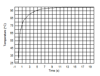
TMP102 Temperature Step ResponseFigure 7-3 Temperature Step Response