ZHCSE86A October 2015 – October 2015 TMP107-Q1
PRODUCTION DATA.
- 1 特性
- 2 应用
- 3 说明
- 4 修订历史记录
- 5 说明(继续)
- 6 Pin Configuration and Functions
- 7 Specifications
-
8 Detailed Description
- 8.1 Overview
- 8.2 Functional Block Diagram
- 8.3 Feature Description
- 8.4 Device Functional Modes
- 8.5 Programming
- 8.6
Register Map
- 8.6.1 Temperature Register (address = 0h) [reset = 0h]
- 8.6.2 Configuration Register (address = 1h) [reset = A000h]
- 8.6.3 High Limit 1 Register (address = 2h) [reset = 7FFCh]
- 8.6.4 Low Limit 1 Register (address = 3h) [reset = 8000h]
- 8.6.5 High Limit 2 Register (address = 4h) [reset = 7FFCh]
- 8.6.6 Low Limit 2 Register (address = 5h) [reset = 8000h]
- 8.6.7 EEPROM n Register (where n = 1 to 8) (addresses = 6h to Dh) [reset = 0h]
- 8.6.8 Die ID Register (address = Fh) [reset = 1107h]
- 9 Application and Implementation
- 10Power Supply Recommendations
- 11Layout
- 12器件和文档支持
- 13机械、封装和可订购信息
9 Application and Implementation
NOTE
Information in the following applications sections is not part of the TI component specification, and TI does not warrant its accuracy or completeness. TI’s customers are responsible for determining suitability of components for their purposes. Customers should validate and test their design implementation to confirm system functionality.
9.1 Application Information
The TMP107-Q1 is a digital temperature sensor that is optimal for thermal monitoring of large areas and over long distances between the host and the sensors. The SMAART-wire interface of the TMP107-Q1 allows for data transfer over a single wire at distances of up to 1000 feet (300 meters) between consecutive devices in the chain.
9.2 Typical Applications
9.2.1 Connecting Multiple Devices
Figure 39 shows typical connections for TMP107-Q1 devices in a daisy-chain configuration.

9.2.1.1 Design Requirements
To avoid any bus contention between the host and the TMP107-Q1 devices, use a tri-state buffer, such as the SN74LVC1G125. Use a 100-Ω resistor (typical) in series with the RX input to limit the amount of current in case of overshoot. A 10-Ω resistor (typical) between the tri-state buffer and the first TMP107-Q1 device reduces any signal collisions between the buffer and the TMP107-Q1 by limiting the amount of current flow. The pullup resistor at the output of the tri-state buffer defines the baud rate of communication. Use a 4.1-kΩ pullup resistor, as shown in Figure 39, to support the entire baud rate range specified in the Timing Requirements. A 0.1-μF bypass capacitor is recommended for each TMP107-Q1 device in the daisy-chain.
9.2.1.2 Detailed Design Procedure
Multiple devices are connected with cables in this typical application. The maximum cable length between two TMP107-Q1 devices can vary because of the effective resistance and capacitance of the type of cable used in a customer application.
9.2.1.2.1 Voltage Drop Effect
Take into account the voltage drop that occurs along the supply and ground lines as a result of the currents of all the devices on the line. This voltage drop occurs as a result of multiple devices simultaneously consuming current through the combined resistance of the common wire, connectors, and solder contacts. Make sure that the supply on the last device does not fall below the minimum operating supply of 1.7 V during any mode of operation, or below 1.8 V during EEPROM programming and chain initialization.
9.2.1.2.2 EEPROM Programming Current
Another parameter to consider is the EEPROM programming current. The device consumes higher current during EEPROM programming than during regular operation, as specified in the Electrical Characteristics section. This higher current consumption results in a larger voltage drop along the supply and ground lines and may lead to similar issues as mentioned previously. To avoid large, simultaneous, programming currents from multiple devices, program the EEPROM on the devices using the individual write commands instead of the global write commands.
9.2.1.2.3 Power Savings
In continuous-conversion mode, the TMP107-Q1 continuously measures temperature and consumes the most power out of any of the operating modes. For maximum power savings, place the TMP107-Q1 in shutdown mode. In shutdown mode, the TMP107-Q1 shuts down all internal active circuitry except for the required circuit elements that allow communication with the device. Issue a one-shot command when in shutdown mode to trigger a single temperature measurement.
9.2.1.2.4 Accuracy
In order to achieve the best temperature accuracy when multiple devices are connected in the daisy-chain, configure the devices in shutdown mode, and then issue a one-shot conversion. Read the temperature from all devices on the bus by issuing a global read after a delay of 20 ms. This delay after the one-shot command makes sure the internal ADC conversion is finished, and the voltages of the supply bypass capacitors over the daisy chain are stable, before the data are read by the host.
9.2.1.2.5 Electromagnetic Interference (EMI)
The typical, three-conductor TMP107-Q1 measurement chain is fairly insensitive to electromagnetic distortions because the supply, ground and signal wires are running in parallel and located in the same cable housing. To help maintain this insensitivity, do not make any additional electric connections at intermediate nodes in the cable, or at the end of the chain of TMP107-Q1 devices.
There can be environmental effects on a TMP107-Q1 cable implementation in the form of conducted emission. The conducted susceptibility of the cable can be investigated if this is a suspected source of interference. Designing for electromagnetic compatibility with the intended operating environment can mitigate interference. There can be radiated emission from the TMP107-Q1 cable implementation that may affect the radiated susceptibility of surrounding equipment. See specification IEC61000-4-3: Testing and measurement techniques - Radiated, radio-frequency, electromagnetic field immunity test for more information on testing for radiated immunity to signals in the 80-MHz to 6-GHz range. Also, see IEC61000-4-6: Testing and measurement techniques - Immunity to conducted disturbances, induced by radio-frequency fields for information on testing for conducted immunity in the 9-kHz to 80-MHz range.
Physical shielding and electrical filtering can mitigate much of the interference into and out of the surrounding environment and electronics. See IEC62153-4-X: Metallic Communication Cable Test Methods for information on determining the screening effectiveness of a metallic cable shield. The thermal conductivity of additional material around the cable implementation can affect the settling time of the TMP107-Q1 at its position in the cable. This thermal conductivity can also reduce the allowable temperature range exposure of the cable implementation depending on the materials chosen. Generally, passive electrical filtering is very effective at suppressing conducted interference. Circuit board components, such as an EMI filter that increases in resistance significantly in response to higher frequency content, are widely available and often easy to implement. Even simple RC and LC filter configurations on transmission lines provide some immunity.
9.2.1.3 Application Curves
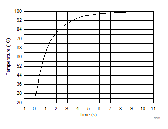
Figure 40 shows the step response of the TMP107-Q1 to a submersion in an oil bath of 100ºC from room temperature (24ºC) at a 3.3-V supply. The time-constant, or the time for the output to reach 63% of the input step, is 1.375 s. The time-constant depends on the printed circuit board (PCB) that the device is mounted on. For this test, the device is soldered to a two-layer PCB that measures 0.551 in × 0.748 in.
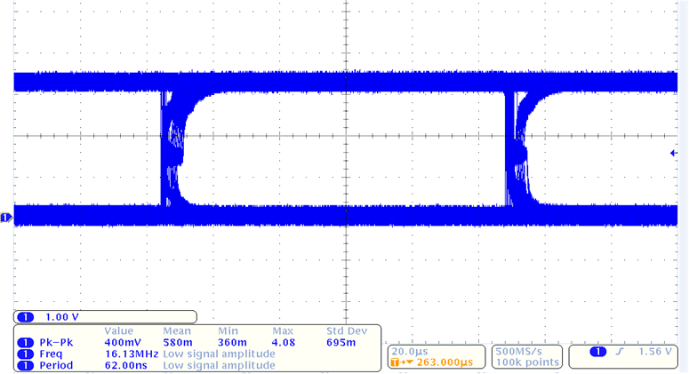
Figure 41 shows the TMP107-Q1 eye diagram as a measure of quality for the transmission path (cable). Measurement of eye patterns is performed by a setup where a source generates a known bit stream that is fed into a transmission channel. The eye diagram of TMP107-Q1 is taken on the I/O line at the far end of a 300-meter cable connecting two TMP107-Q1 devices. The baud rate is 9600 Kbps, and the supply voltage is set to 3.3 V. The scope is set to trigger on I/O rising (or falling) edge, with an infinite persistent time. The superimposed, captured waveforms create the eye diagram. Excellent eye diagram parameters are maintained at 9600 Kbps speed.


9.2.2 Connecting ALERT1 and ALERT2 Pins
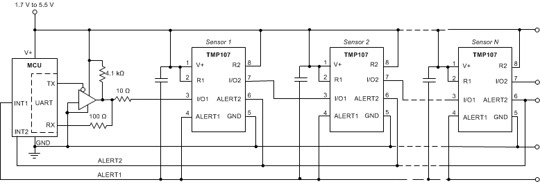
As described in the ALERT1, ALERT2, R1, and R2 Pins section, the TMP107-Q1 contains internal 100-kΩ pullup resistors connected between pins ALERT1 and R1, and pins ALERT2 and R2. Connect R1 and R2 to V+ in order to enable the internal pullup resistors. Figure 42 shows a schematic example of how to connect these pins for multiple TMP107-Q1 devices in a daisy-chain configuration.
 Figure 42. Connecting ALERT1 and ALERT2 Pins
9.2.3 ALERT1 and ALERT2 Pins Used as General-Purpose Output (GPO)
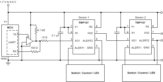
The TMP107-Q1 alert pins are also used as a GPO to control external switches or LEDs. This feature is useful in applications wherein the wiring between general-purpose output lines from the microcontroller or host to a control switch or LED can be eliminated by communicating through the I/O pins of TMP107-Q1. To configure the ALERTx pins as a GPO, program the high-limit register to the highest temperature (7FFCh) and the low-limit register to the lowest temperature (8000h). This programming disables the ALERTx pins from performing high- and low-limit temperature controls. The configuration register polarity bits (POL1 and POL2) are used to toggle the ALERTx pin output. The ALERTx pins are open-drain outputs; therefore, make sure the R1 and R2 pins are connected to the supply voltage, as shown in Figure 43.
 Figure 43. ALERT1 and ALERT2 Pins Used as General-Purpose Output