ZHCSE86A October   2015  – October 2015 TMP107-Q1

PRODUCTION DATA.  

  1. 特性
  2. 应用
  3. 说明
  4. 修订历史记录
  5. 说明(继续)
  6. Pin Configuration and Functions
  7. Specifications
    1. 7.1 Absolute Maximum Ratings
    2. 7.2 ESD Ratings
    3. 7.3 Recommended Operating Conditions
    4. 7.4 Thermal Information
    5. 7.5 Electrical Characteristics
    6. 7.6 Timing Requirements
    7. 7.7 Typical Characteristics
  8. Detailed Description
    1. 8.1 Overview
    2. 8.2 Functional Block Diagram
    3. 8.3 Feature Description
      1. 8.3.1 Digital Temperature Output
      2. 8.3.2 Temperature Limits and Alert
        1. 8.3.2.1 ALERT1, ALERT2, R1, and R2 Pins
      3. 8.3.3 SMAART Wire Communication Interface
        1. 8.3.3.1 Communication Protocol
          1. 8.3.3.1.1 Calibration Phase
          2. 8.3.3.1.2 Command and Address Phase
            1. 8.3.3.1.2.1 Global or Individual (G/nI) Bit
            2. 8.3.3.1.2.2 Read/Write (R/nW) Bit
            3. 8.3.3.1.2.3 Command or Address (C/nA) Bit:
          3. 8.3.3.1.3 Register Pointer Phase
          4. 8.3.3.1.4 Data Phase
        2. 8.3.3.2 SMAART Wire Operations
          1. 8.3.3.2.1 Command Operations
            1. 8.3.3.2.1.1 Address Initialize
            2. 8.3.3.2.1.2 Last Device Poll
            3. 8.3.3.2.1.3 Global Software Reset
          2. 8.3.3.2.2 Address Operations
            1. 8.3.3.2.2.1 Individual Write
            2. 8.3.3.2.2.2 Individual Read
            3. 8.3.3.2.2.3 Global Write
            4. 8.3.3.2.2.4 Global Read
    4. 8.4 Device Functional Modes
      1. 8.4.1 Continuous-Conversion Mode
      2. 8.4.2 Shutdown Mode
      3. 8.4.3 One-Shot Mode
    5. 8.5 Programming
      1. 8.5.1 EEPROM
      2. 8.5.2 EEPROM Operations
        1. 8.5.2.1 EEPROM Unlock
        2. 8.5.2.2 EEPROM Lock
        3. 8.5.2.3 EEPROM Programming
        4. 8.5.2.4 EEPROM Acquire or Read
    6. 8.6 Register Map
      1. 8.6.1 Temperature Register (address = 0h) [reset = 0h]
      2. 8.6.2 Configuration Register (address = 1h) [reset = A000h]
      3. 8.6.3 High Limit 1 Register (address = 2h) [reset = 7FFCh]
      4. 8.6.4 Low Limit 1 Register (address = 3h) [reset = 8000h]
      5. 8.6.5 High Limit 2 Register (address = 4h) [reset = 7FFCh]
      6. 8.6.6 Low Limit 2 Register (address = 5h) [reset = 8000h]
      7. 8.6.7 EEPROM n Register (where n = 1 to 8) (addresses = 6h to Dh) [reset = 0h]
      8. 8.6.8 Die ID Register (address = Fh) [reset = 1107h]
  9. Application and Implementation
    1. 9.1 Application Information
    2. 9.2 Typical Applications
      1. 9.2.1 Connecting Multiple Devices
        1. 9.2.1.1 Design Requirements
        2. 9.2.1.2 Detailed Design Procedure
          1. 9.2.1.2.1 Voltage Drop Effect
          2. 9.2.1.2.2 EEPROM Programming Current
          3. 9.2.1.2.3 Power Savings
          4. 9.2.1.2.4 Accuracy
          5. 9.2.1.2.5 Electromagnetic Interference (EMI)
        3. 9.2.1.3 Application Curves
      2. 9.2.2 Connecting ALERT1 and ALERT2 Pins
      3. 9.2.3 ALERT1 and ALERT2 Pins Used as General-Purpose Output (GPO)
  10. 10Power Supply Recommendations
  11. 11Layout
    1. 11.1 Layout Guidelines
    2. 11.2 Layout Example
  12. 12器件和文档支持
    1. 12.1 文档支持
      1. 12.1.1 相关文档 
    2. 12.2 社区资源
    3. 12.3 商标
    4. 12.4 静电放电警告
    5. 12.5 Glossary
  13. 13机械、封装和可订购信息

封装选项

机械数据 (封装 | 引脚)
散热焊盘机械数据 (封装 | 引脚)
订购信息

11 Layout

11.1 Layout Guidelines

Mount the TMP107-Q1 to a PCB as shown in Figure 44. Obtaining acceptable performance with alternate layout schemes is possible, however this layout produces good results and is intended as a guideline.

  • Bypass the V+ pin to ground with a low-ESR ceramic bypass-capacitor. The typical recommended bypass capacitance is a 0.1-μF ceramic capacitor with a X5R or X7R dielectric. The optimum placement is closest to the V+ and GND pins of the device. Take care to minimize the loop area formed by the bypass-capacitor connection, the V+ pin, and the GND pin of the IC.
  • Use larger copper area pads to reduce self-heating and lower thermal resistance to the environment.
  • If possible, use PCB boards with thick copper layers.
  • If possible, do not use stain to protect the IC because stain can increase thermal resistance.

11.2 Layout Example
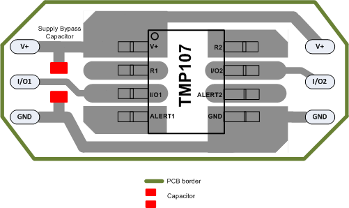
TMP107-Q1 pcblayout_recommendation_sbos716.gif Figure 44. Layout Example