ZHCSE86A October 2015 – October 2015 TMP107-Q1
PRODUCTION DATA.
- 1 特性
- 2 应用
- 3 说明
- 4 修订历史记录
- 5 说明(继续)
- 6 Pin Configuration and Functions
- 7 Specifications
-
8 Detailed Description
- 8.1 Overview
- 8.2 Functional Block Diagram
- 8.3 Feature Description
- 8.4 Device Functional Modes
- 8.5 Programming
- 8.6
Register Map
- 8.6.1 Temperature Register (address = 0h) [reset = 0h]
- 8.6.2 Configuration Register (address = 1h) [reset = A000h]
- 8.6.3 High Limit 1 Register (address = 2h) [reset = 7FFCh]
- 8.6.4 Low Limit 1 Register (address = 3h) [reset = 8000h]
- 8.6.5 High Limit 2 Register (address = 4h) [reset = 7FFCh]
- 8.6.6 Low Limit 2 Register (address = 5h) [reset = 8000h]
- 8.6.7 EEPROM n Register (where n = 1 to 8) (addresses = 6h to Dh) [reset = 0h]
- 8.6.8 Die ID Register (address = Fh) [reset = 1107h]
- 9 Application and Implementation
- 10Power Supply Recommendations
- 11Layout
- 12器件和文档支持
- 13机械、封装和可订购信息
7 Specifications
7.1 Absolute Maximum Ratings
over operating free-air temperature range (unless otherwise noted)(1)| MIN | MAX | UNIT | ||
|---|---|---|---|---|
| Supply voltage, V+ | 6 | V | ||
| Input voltage | I/O1, I/O2 | –0.3 | (V+) + 0.3 | V |
| R1, R2 | –0.3 | 6 | ||
| ALERT1, ALERT2 | –0.3 | 6 | ||
| Sink current | ALERT1, ALERT2 | 10 | mA | |
| Temperature | Operating junction | –55 | 150 | °C |
| Storage, Tstg | –60 | 150 | ||
(1) Stresses beyond those listed under Absolute Maximum Ratings may cause permanent damage to the device. These are stress ratings only, which do not imply functional operation of the device at these or any other conditions beyond those indicated under Recommended Operating Conditions. Exposure to absolute-maximum-rated conditions for extended periods may affect device reliability.
7.2 ESD Ratings
| VALUE | UNIT | |||
|---|---|---|---|---|
| V(ESD) | Electrostatic discharge | Human-body model (HBM), per AEC Q100-002(1) | ±2000 | V |
| Charged-device model (CDM), per AEC Q100-011 | ±1000 | |||
(1) AEC Q100-002 indicates that HBM stressing shall be in accordance with the ANSI/ESDA/JEDEC JS-001 specification.
7.3 Recommended Operating Conditions
over operating free-air temperature range (unless otherwise noted)| MIN | NOM | MAX | UNIT | ||
|---|---|---|---|---|---|
| Supply voltage, V+ | 1.7 | 3.3 | 5.5 | V | |
| Operating free-air temperature, TA | –55 | 125 | °C | ||
7.4 Thermal Information
| THERMAL METRIC(1) | TMP107-Q1 | UNIT | |
|---|---|---|---|
| D (SOIC) | |||
| 8 PINS | |||
| RθJA | Junction-to-ambient thermal resistance | 116.3 | °C/W |
| RθJC(top) | Junction-to-case (top) thermal resistance | 62.5 | °C/W |
| RθJB | Junction-to-board thermal resistance | 56.6 | °C/W |
| ψJT | Junction-to-top characterization parameter | 14.6 | °C/W |
| ψJB | Junction-to-board characterization parameter | 56.0 | °C/W |
| RθJC(bot) | Junction-to-case (bottom) thermal resistance | N/A | °C/W |
(1) For more information about traditional and new thermal metrics, see the Semiconductor and IC Package Thermal Metrics application report, SPRA953.
7.5 Electrical Characteristics
At TA = –55°C to 125°C and V+ = +1.7 V to +5.5 V (unless otherwise noted). Typical values at TA = 25°C and V+ = 3.3 V.| PARAMETER | TEST CONDITIONS | MIN | TYP | MAX | UNIT | |
|---|---|---|---|---|---|---|
| TEMPERATURE INPUT | ||||||
| Temperature range | –55 | 125 | °C | |||
| Temperature resolution | 0.015625 | °C | ||||
| Temperature accuracy (error) | –20°C to +70°C; one-shot mode, bus inactive | ±0.125 | ±0.4 | °C | ||
| –40°C to +100°C; one-shot mode, bus inactive | ±0.125 | ±0.55 | ||||
| –55°C to +125°C; one-shot mode, bus inactive | ±0.5 | ±0.7 | ||||
| ADC resolution | 14 | Bits | ||||
| DIGITAL OUTPUT (ALERT1, ALERT2) | ||||||
| VOL | Low-level output voltage | IOUT = –1 mA | 0 | 0.02 | 0.4 | V |
| IOH | High-level output leakage current | VO = V+ | 0.1 | 1 | μA | |
| RPU | Pullup resistors | 75 | 100 | 125 | kΩ | |
| DIGITAL INPUT/OUTPUT (I/O1, I/O2) | ||||||
| VIH | High-level input voltage | 0.7 (V+) | (V+) + 0.3 | V | ||
| VIL | Low-level input voltage | –0.3 | 0.3 (V+) | V | ||
| IIN | Input current | 0 V < VIN < (V+) + 0.3 V | –1 | 1 | μA | |
| VOL | Low-level output voltage | IOUT = –1 mA | 0 | 0.1 | 0.4 | V |
| VOH | High-level output voltage | IOUT = 1 mA | (V+) – 0.4 | (V+) – 0.1 | V+ | V |
| Short-circuit current | Short-circuit I/O1 and I/O2 to ground or V+, V+ = 5 V |
60 | mA | |||
| DEVICE TIMING | ||||||
| Conversion time | One-shot mode | 12 | 15 | 18 | ms | |
| Conversion rate | Programmable | 1/16 | 62 | Conv/s | ||
| Device timeout time | Any communication | 35 | 40 | ms | ||
| Global address-initialize command | 1 | 1.25 | s | |||
| EEPROM | ||||||
| Programming time | V+ > 1.8 V | 7 | ms | |||
| Number of writes | V+ > 1.8 V | 1000 | 100,000 | Times | ||
| Data retention time | 10 | Years | ||||
| POWER SUPPLY | ||||||
| V+ | Operating supply range | 1.7 | 3.3 | 5.5 | V | |
| EEPROM write | 1.8 | 3.3 | 5.5 | V | ||
| IQ | Quiescent current | ADC conversion on, SMAART wire bus inactive |
200 | 400 | μA | |
| ADC conversion on, SMAART wire bus active (bus baud rate = 57.6 kBd) | 300 | |||||
| ADC conversion off, SMAART wire bus active (bus baud rate = 57.6 kBd) | 100 | |||||
| 1 conversion per second average, SMAART wire bus inactive |
16 | 35 | ||||
| EEPROM write (ADC conversion off) | 400 | |||||
| ISD | Shutdown current | SMAART wire bus inactive (I/O1, I/O2 = V+) | 3.8 | 10 | μA | |
| Power-on reset voltage | Supply voltage rising | 1.4 | V | |||
7.6 Timing Requirements
| MIN | NOM | MAX | UNIT | ||
|---|---|---|---|---|---|
| FROM HOST TO THE TMP107-Q1 | |||||
| 1/tBAUD | SMAART bus baud rate | 4.8 | 115.4 | kBd | |
| tRISE + tJITTER | SMAART bus transition from low to high + edge timing variance | 15 | % of (1/baud) | ||
| tFALL + tJITTER | SMAART bus transition from high to low + edge timing variance | 15 | % of (1/baud) | ||
| FROM THE TMP107-Q1 TO HOST OR NEXT TMP107-Q1 IN DAISY-CHAIN | |||||
| tJITTER | Edge timing variance | 1 | µs | ||
| tSKEW | Average phase shift between IO1 and IO2 | 33 | ns | ||
| tRISE | SMAART bus transition from low to high, 10-pF load | 10 | ns | ||
| tFALL | SMAART bus transition from high to low, 10-pF load | 10 | ns | ||
 Figure 1. Timing Diagram
7.7 Typical Characteristics
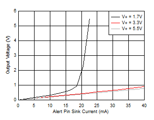
at TA = 25°C and V+ = 3.3 V (unless otherwise noted)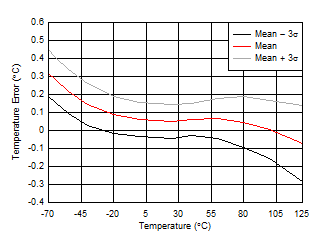
| One-shot mode, specified from –55ºC to +125ºC only |
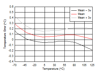
| One-shot mode, V+ = 1.7 V, specified from –55ºC to +125ºC only | ||
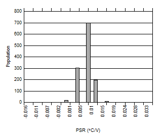
| One-shot mode, V+ = 1.7 V to 5.5 V |
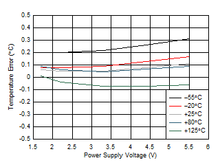
| One-shot mode |
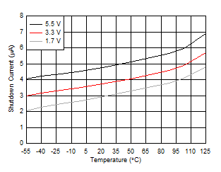
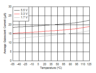
| 1 conversion per second |
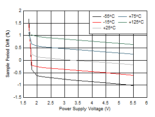
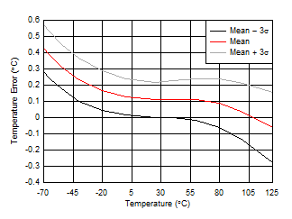
| One-shot mode, V+ = 5.5 V, specified from –55ºC to +125ºC only |
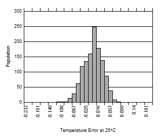
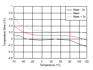
| Continuous-conversion mode, maximum conversion rate, |
| bus inactive |
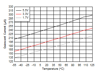
| No bus communication |
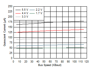
| Shutdown mode |
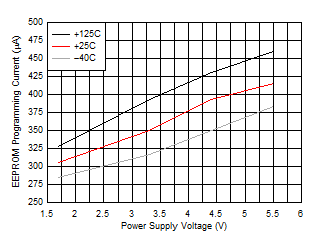
vs Power Supply Voltage
