ZHCSE08D May   2015  – January 2020 TMP107

PRODUCTION DATA.  

  1. 特性
  2. 应用范围
  3. 说明
    1.     Device Images
      1.      典型应用
  4. 修订历史记录
  5. Pin Configuration and Functions
    1.     Pin Functions
  6. Specifications
    1. 6.1 Absolute Maximum Ratings
    2. 6.2 ESD Ratings
    3. 6.3 Recommended Operating Conditions
    4. 6.4 Thermal Information
    5. 6.5 Electrical Characteristics
    6. 6.6 Timing Requirements
    7. 6.7 Typical Characteristics
  7. Detailed Description
    1. 7.1 Overview
    2. 7.2 Functional Block Diagram
    3. 7.3 Feature Description
      1. 7.3.1 Digital Temperature Output
      2. 7.3.2 Temperature Limits and Alert
        1. 7.3.2.1 ALERT1, ALERT2, R1, and R2 Pins
      3. 7.3.3 SMAART Wire™ Communication Interface
        1. 7.3.3.1 Communication Protocol
          1. 7.3.3.1.1 Calibration Phase
          2. 7.3.3.1.2 Command and Address Phase
            1. 7.3.3.1.2.1 Global or Individual (G/nI) Bit
            2. 7.3.3.1.2.2 Read/Write (R/nW) Bit
            3. 7.3.3.1.2.3 Command or Address (C/nA) Bit:
          3. 7.3.3.1.3 Register Pointer Phase
          4. 7.3.3.1.4 Data Phase
        2. 7.3.3.2 SMAART Wire™ Operations
          1. 7.3.3.2.1 Command Operations
            1. 7.3.3.2.1.1 Address Initialize
            2. 7.3.3.2.1.2 Last Device Poll
            3. 7.3.3.2.1.3 Global Software Reset
          2. 7.3.3.2.2 Address Operations
            1. 7.3.3.2.2.1 Individual Write
            2. 7.3.3.2.2.2 Individual Read
            3. 7.3.3.2.2.3 Global Write
            4. 7.3.3.2.2.4 Global Read
    4. 7.4 Device Functional Modes
      1. 7.4.1 Continuous-Conversion Mode
      2. 7.4.2 Shutdown Mode
      3. 7.4.3 One-Shot Mode
    5. 7.5 Programming
      1. 7.5.1 EEPROM
      2. 7.5.2 EEPROM Operations
        1. 7.5.2.1 EEPROM Unlock
        2. 7.5.2.2 EEPROM Lock
        3. 7.5.2.3 EEPROM Programming
        4. 7.5.2.4 EEPROM Acquire or Read
    6. 7.6 Register Map
      1. 7.6.1 Temperature Register (address = 0h) [reset = 0h]
        1. Table 4. Temperature Register Field Descriptions
      2. 7.6.2 Configuration Register (address = 1h) [reset = A000h]
        1. Table 5. Configuration Register Field Descriptions
      3. 7.6.3 High Limit 1 Register (address = 2h) [reset = 7FFCh]
        1. Table 7. High Limit 1 Register Field Descriptions
      4. 7.6.4 Low Limit 1 Register (address = 3h) [reset = 8000h]
        1. Table 8. Low Limit 1 Register Field Descriptions
      5. 7.6.5 High Limit 2 Register (address = 4h) [reset = 7FFCh]
        1. Table 9. High Limit 2 Register Field Descriptions
      6. 7.6.6 Low Limit 2 Register (address = 5h) [reset = 8000h]
        1. Table 10. Low Limit 2 Register Field Descriptions
      7. 7.6.7 EEPROM n Register (where n = 1 to 8) (addresses = 6h to Dh) [reset = 0h]
        1. Table 11. EEPROM Register bits
      8. 7.6.8 Die ID Register (address = Fh) [reset = 1107h]
        1. Table 12. Die ID Register Field Descriptions
  8. Application and Implementation
    1. 8.1 Application Information
    2. 8.2 Typical Applications
      1. 8.2.1 Connecting Multiple Devices
        1. 8.2.1.1 Design Requirements
        2. 8.2.1.2 Detailed Design Procedure
          1. 8.2.1.2.1 Voltage Drop Effect
          2. 8.2.1.2.2 EEPROM Programming Current
          3. 8.2.1.2.3 Power Savings
          4. 8.2.1.2.4 Accuracy
          5. 8.2.1.2.5 Electromagnetic Interference (EMI)
        3. 8.2.1.3 Application Curves
      2. 8.2.2 Connecting ALERT1 and ALERT2 Pins
      3. 8.2.3 ALERT1 and ALERT2 Pins Used as General-Purpose Output (GPO)
  9. Power Supply Recommendations
  10. 10Layout
    1. 10.1 Layout Guidelines
    2. 10.2 Layout Example
  11. 11器件和文档支持
    1. 11.1 文档支持
      1. 11.1.1 相关文档
    2. 11.2 接收文档更新通知
    3. 11.3 社区资源
    4. 11.4 商标
    5. 11.5 静电放电警告
    6. 11.6 Glossary
  12. 12机械、封装和可订购信息

封装选项

机械数据 (封装 | 引脚)
散热焊盘机械数据 (封装 | 引脚)
订购信息

Command or Address (C/nA) Bit:

The C/nA bit indicates whether the current communication is a command operation or address operation. The C/nA bit = 1 indicates a command operation. The codes for specific commands in the TMP107 are listed in Table 2. Codes other than those listed in Table 2 are reserved for factory use only.

The C/nA bit = 0 indicates an address operation. The five bits following the C/nA bit (A4 to A0) are the address bits of the device or devices that the host intends to communicate with in the chain, as shown in Figure 20.
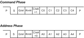
TMP107 cmnd_addr_phase_sbos716.gifFigure 20. Command and Address Phase