ZHCSH80E September   2017  – May 2019 TMP235 , TMP236

PRODUCTION DATA.  

  1. 特性
  2. 应用
  3. 说明
    1.     Device Images
      1.      功能方框图
      2.      输出电压与环境温度间的关系
  4. 修订历史记录
  5. Pin Configuration and Functions
    1.     Pin Functions
  6. Specifications
    1. 6.1 Absolute Maximum Ratings
    2. 6.2 ESD Ratings
    3. 6.3 Recommended Operating Conditions
    4. 6.4 Thermal Information
    5. 6.5 Electrical Characteristics
    6. 6.6 Typical Characteristics
  7. Detailed Description
    1. 7.1 Overview
    2. 7.2 Functional Block Diagram
    3. 7.3 Feature Description
    4. 7.4 Device Functional Modes
  8. Application and Implementation
    1. 8.1 Application Information
    2. 8.2 Typical Application
      1. 8.2.1 Connection to an ADC
        1. 8.2.1.1 Design Requirements
        2. 8.2.1.2 Detailed Design Procedure
        3. 8.2.1.3 Application Curve
  9. Power Supply Recommendations
  10. 10Layout
    1. 10.1 Layout Guidelines
    2. 10.2 Layout Examples
  11. 11器件和文档支持
    1. 11.1 相关链接
    2. 11.2 接收文档更新通知
    3. 11.3 社区资源
    4. 11.4 商标
    5. 11.5 静电放电警告
    6. 11.6 Glossary
  12. 12机械、封装和可订购信息

封装选项

机械数据 (封装 | 引脚)
散热焊盘机械数据 (封装 | 引脚)
订购信息

Typical Characteristics

at TA = 25°C, (unless otherwise noted)
TMP235 TMP236 D001_SBOS857.gif
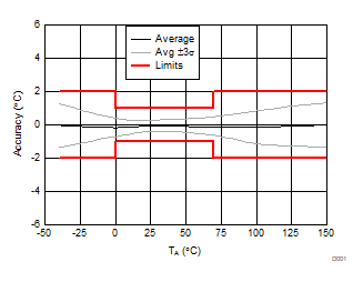
TMP235: VDD = 2.3 to 5.5 V, IOUT = 0 µA, CLOAD = 1000 pF
Figure 1. Accuracy vs. TA Temperature (A2 Accuracy Level)
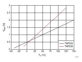
TMP235 TMP236 D003_SBOS857.gif
IOUT = 0 µA, CLOAD = 1000 pF
Figure 3. Output Voltage vs. Ambient Temperature
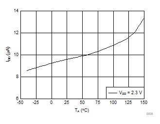
TMP235 TMP236 D005_SBOS857.gif
TMP235: IOUT = 0 µA, CLOAD = 1000 pF
Figure 5. Supply Current vs. Temperature
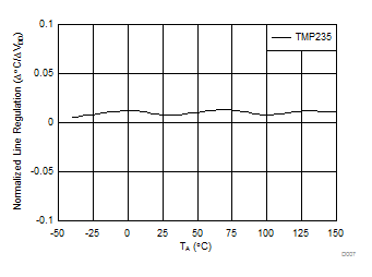
TMP235 TMP236 D007_SBOS857.gif
TMP235: VDD = 2.3 to 5.5 V, IOUT = 0 µA, CLOAD = 1000 pF
Figure 7. Line Regulation (Δ°C / ΔVDD) vs. Ambient Temperature
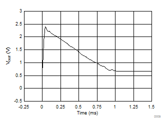
TMP235 TMP236 D009_SBOS857.gif
TMP235: TA = 25°C
Figure 9. Output vs. Settling Time to Step VDD
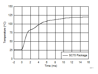
TMP235 TMP236 D011_SBOS857.gif
TMP235: 1 × 1 (inches) PCB, Air 26°C to Fluid Bath 123°C
Figure 11. Thermal Response (Air-to-Fluid Bath)
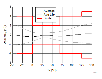
TMP235 TMP236 D002_SBOS857.gif
TMP235: VDD = 2.3 to 5.5 V, IOUT = 0 µA, CLOAD = 1000 pF
Figure 2. Accuracy vs. TA Temperature (A4 Accuracy Level)
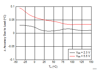
TMP235 TMP236 D004_SBOS857.gif
TMP235: IOUT = from 0 µA to 100 µA, CLOAD = 1000 pF
Figure 4. Changes in Accuracy vs. Ambient Temperature (Due to Load)
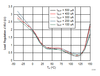
TMP235 TMP236 D006_SBOS857.gif
TMP235: VDD = 2.3 V, CLOAD = 1000 pF
Figure 6. Load Regulation vs. Ambient Temperature
TMP235 TMP236 D008_SBOS857.gif
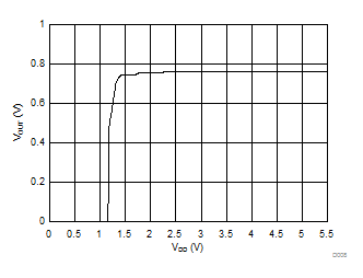
TMP235: TA = 25°C
Figure 8. Output Voltage vs. Power Supply
TMP235 TMP236 D010_SBOS857.gif
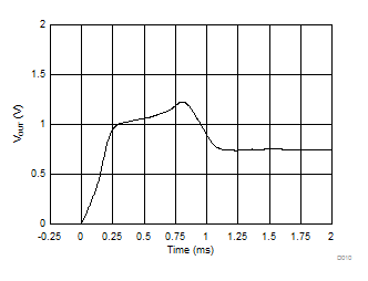
TMP235: TA = 25°C, VDD Ramp Rate = 5 V/ms
Figure 10. Output vs. Settling Time to Ramp VDD
TMP235 TMP236 D012_SBOS857.gif
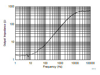
TMP235: TA = 25°C, VDD = 5 V, IOUT = 100 µA
Figure 12. Output Impedance vs. Frequency