ZHCSEG0B November   2015  – April 2017 TMP275-Q1

PRODUCTION DATA.  

  1. 特性
  2. 应用
  3. 说明
  4. 修订历史记录
  5. Pin Configuration and Functions
  6. Specifications
    1. 6.1 Absolute Maximum Ratings
    2. 6.2 ESD Ratings
    3. 6.3 Recommended Operating Conditions
    4. 6.4 Thermal Information
    5. 6.5 Electrical Characteristics
    6. 6.6 Timing Requirements
    7. 6.7 Typical Characteristics
  7. Detailed Description
    1. 7.1 Overview
    2. 7.2 Functional Block Diagram
    3. 7.3 Feature Description
      1. 7.3.1 Digital Temperature Output
      2. 7.3.2 Serial Interface
      3. 7.3.3 Bus Overview
      4. 7.3.4 Serial Bus Address
        1. 7.3.4.1 Writing and Reading to the TMP275-Q1
        2. 7.3.4.2 Slave Mode Operations
          1. 7.3.4.2.1 Slave Receiver Mode
          2. 7.3.4.2.2 Slave Transmitter Mode
        3. 7.3.4.3 SMBus Alert Function
        4. 7.3.4.4 General Call
        5. 7.3.4.5 High-Speed Mode
        6. 7.3.4.6 Time-Out Function
      5. 7.3.5 Timing Diagrams
        1. 7.3.5.1 Two-Wire Timing Diagrams
    4. 7.4 Device Functional Modes
      1. 7.4.1 Shutdown Mode (SD)
      2. 7.4.2 Thermostat Mode (TM)
        1. 7.4.2.1 Comparator Mode (TM = 0)
        2. 7.4.2.2 Interrupt Mode (TM = 1)
      3. 7.4.3 One-Shot (OS)
    5. 7.5 Programming
      1. 7.5.1 Pointer Register
      2. 7.5.2 Temperature Register
      3. 7.5.3 Configuration Register
      4. 7.5.4 Polarity (POL)
      5. 7.5.5 Fault Queue (F1/F0)
      6. 7.5.6 Converter Resolution (R1/R0)
      7. 7.5.7 High- and Low-Limit Registers
  8. Application and Implementation
    1. 8.1 Application Information
    2. 8.2 Typical Applications
      1. 8.2.1 Typical Connections of the TMP275-Q1
        1. 8.2.1.1 Design Requirements
        2. 8.2.1.2 Detailed Design Procedure
        3. 8.2.1.3 Application Curve
      2. 8.2.2 Connecting Multiple Devices on a Single Bus
      3. 8.2.3 Temperature Data Logger for Cold Chain Management Applications
  9. Power Supply Recommendations
  10. 10Layout
    1. 10.1 Layout Guidelines
    2. 10.2 Layout Example
  11. 11器件和文档支持
    1. 11.1 文档支持
      1. 11.1.1 相关文档
    2. 11.2 接收文档更新通知
    3. 11.3 社区资源
    4. 11.4 商标
    5. 11.5 静电放电警告
    6. 11.6 Glossary
  12. 12机械、封装和可订购信息

封装选项

机械数据 (封装 | 引脚)
散热焊盘机械数据 (封装 | 引脚)
订购信息

Pin Configuration and Functions

D, DGK Packages
8-Pin SOIC, VSSOP
Top View
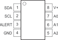
TMP275-Q1 po_bos363d.gif

Pin Functions

PIN I/O DESCRIPTION
NO. NAME
1 SDA I/O Serial data. Open-drain output; requires a pullup resistor.
2 SCL I Serial clock. Open-drain output; requires a pullup resistor.
3 ALERT O Overtemperature alert. Open-drain output; requires a pullup resistor.
4 GND Ground
5 A2 I Address select. Connect to GND or V+.
6 A1 I
7 A0 I
8 V+ I Supply voltage, 2.7 V to 5.5 V