ZHCSCZ4C October   2014  – September 2018 TMP302-Q1

PRODUCTION DATA.  

  1. 特性
  2. 应用
  3. 说明
    1.     Device Images
      1.      跳变阈值精度
  4. 修订历史记录
  5. 器件比较表
  6. Pin Configuration and Functions
    1.     Pin Functions
  7. Specifications
    1. 7.1 Absolute Maximum Ratings
    2. 7.2 ESD Ratings
    3. 7.3 Recommended Operating Conditions
    4. 7.4 Thermal Information
    5. 7.5 Electrical Characteristics
    6. 7.6 Typical Characteristics
  8. Detailed Description
    1. 8.1 Overview
    2. 8.2 Functional Block Diagram
    3. 8.3 Feature Description
      1. 8.3.1 HYSTSET
    4. 8.4 Device Functional Modes
  9. Application and Implementation
    1. 9.1 Application Information
      1. 9.1.1 Configuring the TMP302-Q1
    2. 9.2 Typical Application
      1. 9.2.1 Design Requirements
      2. 9.2.2 Detailed Design Procedure
      3. 9.2.3 Application Curves
  10. 10Power Supply Recommendations
  11. 11Layout
    1. 11.1 Layout Guidelines
    2. 11.2 Layout Example
  12. 12器件和文档支持
    1. 12.1 接收文档更新通知
    2. 12.2 社区资源
    3. 12.3 商标
    4. 12.4 静电放电警告
    5. 12.5 术语表
  13. 13机械、封装和可订购信息

封装选项

机械数据 (封装 | 引脚)
散热焊盘机械数据 (封装 | 引脚)
订购信息

Application Curves

Figure 12 and Figure 13 show the TMP302A-Q1 power-on response with the ambient temperature less than 50°C and greater than 50°C respectively. The TMP302A-Q1 was configured with trip point set to 50°C. The TMP302B-Q1, TMP302C-Q1, and TMP302D-Q1 devices behave similarly with regards to power on response with TA below or above the trip point. Note that the OUT signal typically requires 35 ms following power on to become valid.

TMP302-Q1 TMP302AQ1_Power_On_Ta_LT_50_SLOS889.gifFigure 12. TMP302A-Q1 Power-On Response,
TA Less than 50°C
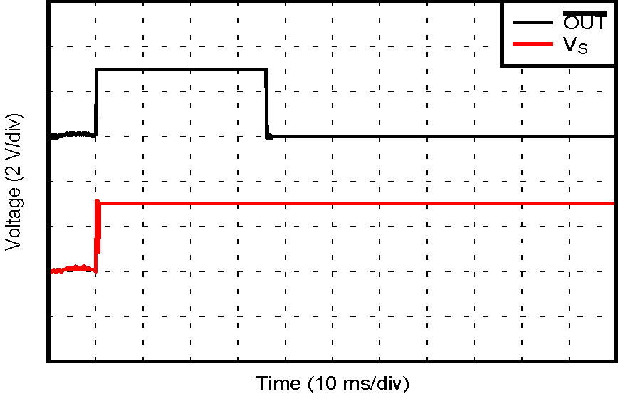
TMP302-Q1 TMP302AQ1_Power_On_Ta_GT_50_SLOS889.gifFigure 13. TMP302A-Q1 Power-On Response,
TA Greater than 50°C