SBOS371B August   2006  – October 2014 TMP401

PRODUCTION DATA.  

  1. Features
  2. Applications
  3. Description
  4. Revision History
  5. Pin Configuration and Functions
  6. Specifications
    1. 6.1 Absolute Maximum Ratings
    2. 6.2 Handling Ratings
    3. 6.3 Recommended Operating Conditions
    4. 6.4 Thermal Information
    5. 6.5 Electrical Characteristics: V+ = 3 V to 5.5 V
    6. 6.6 Timing Requirements
    7. 6.7 Typical Characteristics
  7. Detailed Description
    1. 7.1 Overview
    2. 7.2 Functional Block Diagram
    3. 7.3 Feature Description
      1. 7.3.1 Standard and Extended Temperature Measurement Range
      2. 7.3.2 Remote Sensing
    4. 7.4 Device Functional Modes
      1. 7.4.1 SMBus Alert Function
      2. 7.4.2 THERM (Pin 4) and ALERT/THERM2 (Pin 6)
      3. 7.4.3 Sensor Fault
      4. 7.4.4 High-Speed Mode
      5. 7.4.5 Shutdown Mode (SD)
      6. 7.4.6 One-Shot Conversion
      7. 7.4.7 General-Call Reset
    5. 7.5 Programming
      1. 7.5.1 Bus Overview
      2. 7.5.2 Serial Interface
      3. 7.5.3 Serial Bus Address
      4. 7.5.4 Read and Write Operations
      5. 7.5.5 Timeout Function
      6. 7.5.6 Timing Diagrams
    6. 7.6 Register Maps
      1. 7.6.1  Pointer Register
      2. 7.6.2  Temperature Registers
      3. 7.6.3  Limit Registers
      4. 7.6.4  Status Register
      5. 7.6.5  Configuration Register
      6. 7.6.6  Resolution Register
      7. 7.6.7  Conversion Rate Register
      8. 7.6.8  Identification Registers
      9. 7.6.9  Consecutive Alert Register
      10. 7.6.10 THERM Hysteresis Register
  8. Application and Implementation
    1. 8.1 Application Information
    2. 8.2 Typical Application
      1. 8.2.1 Design Requirements
      2. 8.2.2 Detailed Design Procedure
        1. 8.2.2.1 Filtering
      3. 8.2.3 Application Curves
        1. 8.2.3.1 Series Resistance Cancellation
        2. 8.2.3.2 Differential Input Capacitance
  9. Power-Supply Recommendations
  10. 10Layout
    1. 10.1 Layout Guidelines
      1. 10.1.1 Measurement Accuracy and Thermal Considerations
      2. 10.1.2 Layout Considerations
    2. 10.2 Layout Examples
  11. 11Device and Documentation Support
    1. 11.1 Trademarks
    2. 11.2 Electrostatic Discharge Caution
    3. 11.3 Glossary
  12. 12Mechanical, Packaging, and Orderable Information

封装选项

机械数据 (封装 | 引脚)
散热焊盘机械数据 (封装 | 引脚)
订购信息

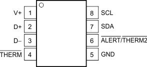
5 Pin Configuration and Functions

DGK Package
VSSOP-8
(Top View)
po_sbos371.gif

Pin Functions

PIN I/O DESCRIPTION
NO. NAME
1 V+ Analog input Positive supply (3 V to 5.5 V)
2 D+ Analog input Positive connection to remote temperature sensor
3 D– Analog input Negative connection to remote temperature sensor
4 THERM Digital output Thermal flag, active low, open-drain; requires pull-up resistor to V+
5 GND Ground
6 ALERT/THERM2 Digital output Alert (reconfigurable as second thermal flag), active low, open-drain; requires pull-up resistor to V+
7 SDA Digital I/O Serial data line for SMBus, open-drain; requires pull-up resistor to V+
8 SCL Digital I/O Serial clock line for SMBus, open-drain; requires pull-up resistor to V+