ZHCSFV7 November 2016 TMP421-Q1 , TMP422-Q1 , TMP423-Q1
PRODUCTION DATA.
- 1 特性
- 2 应用
- 3 说明
- 4 修订历史记录
- 5 Device Comparison Table
- 6 Pin Configuration and Functions
- 7 Specifications
-
8 Detailed Description
- 8.1 Overview
- 8.2 Functional Block Diagram
- 8.3 Feature Description
- 8.4 Device Functional Modes
- 8.5
Programming
- 8.5.1 Serial Interface
- 8.5.2 Bus Overview
- 8.5.3 Bus Definitions
- 8.5.4 Serial Bus Address
- 8.5.5 Two-Wire Interface Slave Device Addresses
- 8.5.6 Read and Write Operations
- 8.5.7 High-Speed Mode
- 8.5.8 One-Shot Conversion
- 8.5.9 η-Factor Correction Register
- 8.5.10 Software Reset
- 8.5.11 General Call Reset
- 8.5.12 Identification Registers
- 8.6 Register Maps
- 9 Application and Implementation
- 10Power Supply Recommendations
- 11Layout
- 12器件和文档支持
- 13机械、封装和可订购信息
7 Specifications
7.1 Absolute Maximum Ratings
over operating free-air temperature range (unless otherwise noted)(1)| MIN | MAX | UNIT | ||
|---|---|---|---|---|
| Power supply, VS | 7 | V | ||
| Input voltage | Pins 1, 2, 3, and 4 only | –0.5 | VS + 0.5 | V |
| Pins 6 and 7 only | –0.5 | 7 | ||
| Input current | 10 | mA | ||
| Operational temperature | –55 | 127 | °C | |
| Junction temperature, TJ max | 150 | °C | ||
| Storage temperature, Tstg | –60 | 130 | °C | |
(1) Stresses beyond those listed under Absolute Maximum Ratings may cause permanent damage to the device. These are stress ratings only, which do not imply functional operation of the device at these or any other conditions beyond those indicated under Recommended Operating Conditions. Exposure to absolute-maximum-rated conditions for extended periods may affect device reliability.
7.2 ESD Ratings
| VALUE | UNIT | |||
|---|---|---|---|---|
| V(ESD) | Electrostatic discharge | Human-body model (HBM), per AEC Q100-002(1) | ±3000 | V |
| Charged-device model (CDM), per AEC Q100-011 | ±750 | |||
(1) AEC Q100-002 indicates that HBM stressing shall be in accordance with the ANSI/ESDA/JEDEC JS-001 specification.
7.3 Recommended Operating Conditions
over operating free-air temperature range (unless otherwise noted)| MIN | MAX | UNIT | ||
|---|---|---|---|---|
| Temperature | –40 | 125 | °C | |
| Power-supply voltage | 2.7 | 5.5 | V | |
7.4 Thermal Information
| THERMAL METRIC(1) | TMP42x-Q1 | UNIT | |
|---|---|---|---|
| DCN (SOT-23) | |||
| 8 PINS | |||
| RθJA | Junction-to-ambient thermal resistance | 147 | °C/W |
| RθJC(top) | Junction-to-case (top) thermal resistance | 115 | °C/W |
| RθJB | Junction-to-board thermal resistance | 33 | °C/W |
| ψJT | Junction-to-top characterization parameter | 38 | °C/W |
| ψJB | Junction-to-board characterization parameter | 33 | °C/W |
(1) For more information about traditional and new thermal metrics, see the Semiconductor and IC Package Thermal Metrics application report.
7.5 Electrical Characteristics
at TA = –40°C to +125°C and V+ = 2.7 V to 5.5 V (unless otherwise noted)| PARAMETER | TEST CONDITIONS | MIN | TYP | MAX | UNIT | |
|---|---|---|---|---|---|---|
| TEMPERATURE ERROR | ||||||
| TELOCAL | Local temperature sensor | TA = –40°C to +125°C | –2.5 | ±1.25 | 2.5 | °C |
| TA = 15°C to 85°C, V+ = 3.3 V | –1.5 | ±0.25 | 1.5 | |||
| TEREMOTE | Remote temperature sensor(1) | TA = 15°C to 85°C, TD = –40°C to +150°C, V+ = 3.3 V | –1 | ±0.25 | 1 | °C |
| TA = –40°C to +100°C, TD = –40°C to +150°C, V+ = 3.3 V | –3 | ±1 | 3 | |||
| TA = –40°C to +125°C, TD = –40°C to +150°C | –5 | ±3 | 5 | |||
| PSS | Local and remote power-supply sensitivity | V+ = 2.7 V to 5.5 V | –0.5 | ±0.2 | 0.5 | °C/V |
| TEMPERATURE MEASUREMENT | ||||||
| Conversion time (per channel) | 100 | 115 | 130 | ms | ||
| Resolution | Local temperature sensor (programmable) | 12 | Bits | |||
| Remote temperature sensor | 12 | |||||
| Remote sensor source currents | High, series resistance = 3 kΩ maximum | 120 | μA | |||
| Medium high | 60 | |||||
| Medium low | 12 | |||||
| Low | 6 | |||||
| η | Remote transistor ideality factor | TMP42x-Q1 optimized ideality factor | 1.008 | |||
| SMBus INTERFACE | ||||||
| VIH | Logic input high voltage (SCL, SDA) | 2.1 | V | |||
| VIL | Logic input low voltage (SCL, SDA) | 0.8 | V | |||
| Hysteresis | 500 | mV | ||||
| SMBus output low sink current | 6 | mA | ||||
| VOL | SDA output low voltage | IOUT = 6 mA | 0.15 | 0.4 | V | |
| Logic input current | 0 ≤ VIN ≤ 6 V | –1 | 1 | μA | ||
| DIGITAL INPUTS | ||||||
| Input capacitance | 3 | pF | ||||
| VIH | Input logic high voltage | 0.7(V+) | (V+)+0.5 | V | ||
| VIL | Input logic low voltage | –0.5 | 0.3(V+) | V | ||
| IIN | Leakage input current | 0 V ≤ VIN ≤ V+ | 1 | μA | ||
| POWER SUPPLY | ||||||
| V+ | Specified voltage range | 2.7 | 5.5 | V | ||
| IQ | Quiescent current | 0.0625 conversions per second | 32 | 38 | μA | |
| Eight conversions per second | 400 | 525 | μA | |||
| Serial bus inactive, shutdown mode | 3 | 10 | μA | |||
| Serial bus active, fS = 400 kHz, shutdown mode | 90 | μA | ||||
| Serial bus active, fS = 3.4 MHz, shutdown mode | 350 | μA | ||||
| UVLO | Undervoltage lockout | 2.3 | 2.4 | 2.6 | V | |
| POR | Power-on-reset threshold | 1.6 | 2.3 | V | ||
(1) Tested with less than 5-Ω effective series resistance and 100-pF differential input capacitance.
7.6 Timing Requirements
at –40°C to +125°C and V+ = 2.7 V to 5.5 V (unless otherwise noted); values are based on statistical analysis of samples tested during initial release| FAST MODE | HIGH-SPEED MODE | UNIT | ||||
|---|---|---|---|---|---|---|
| MIN | MAX | MIN | MAX | |||
| f(SCL) | SCL operating frequency | 0.001 | 0.4 | 0.001 | 2.56 | MHz |
| t(BUF) | Bus free time between STOP and START condition | 1300 | 160 | ns | ||
| t(HD;STA) | Hold time after repeated START condition. After this period, the first clock is generated. |
600 | 160 | ns | ||
| t(SU;STA) | Repeated START condition setup time | 600 | 160 | ns | ||
| t(SU;STO) | STOP condition setup time | 600 | 160 | ns | ||
| t(HD;DAT) | Data hold time | 25 | See (1) | 5 | 90 | ns |
| t(VD.DAT) | Data valid time (data response time)(2) | 900 | Not applicable | ns | ||
| t(SU;DAT) | Data setup time | 100 | 10 | ns | ||
| t(LOW) | SCL clock LOW period | 1300 | 250 | ns | ||
| t(HIGH) | SCL clock HIGH period | 600 | 60 | ns | ||
| tF – SDA | Data fall time | 300 | 150 | ns | ||
| tF – SCL | Clock fall time | 300 | 40 | ns | ||
| tR | Clock, data rise time | 1000 | ns | |||
| Serial bus timeout | 25 | 35 | 25 | 35 | ms | |
(1) The maximum tHD;DAT can be 0.9 μs for Fast-Mode, and is less than the maximum tVD;DAT by a transition time.
(2) tVDDATA = time for data signal from SCL LOW to SDA output (HIGH to LOW, depending on which is worse).
 Figure 1. Two-Wire Timing Diagram
7.7 Typical Characteristics
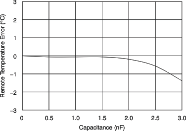
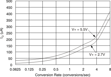
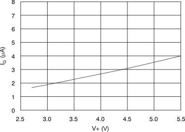
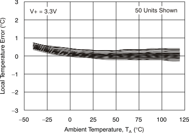
at TA = 25°C and V+ = 5 V (unless otherwise noted)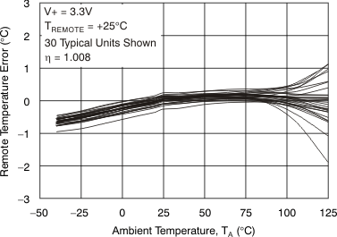
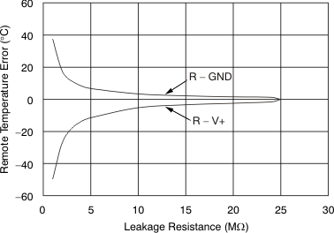
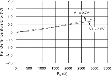
(GND Collector-Connected Transistor, 2N3906 PNP)
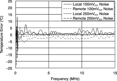
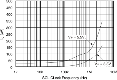
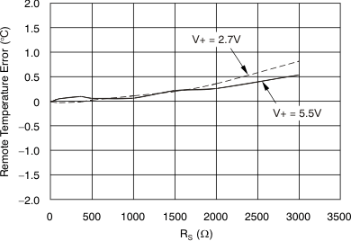
(Diode-Connected Transistor, 2N3906 PNP)
