ZHCSCV4C October 2014 – April 2021 TMP451-Q1
PRODUCTION DATA
- 1 特性
- 2 应用
- 3 说明
- 4 Revision History
- 5 Pin Configuration and Functions
- 6 Specifications
-
7 Detailed Description
- 7.1 Overview
- 7.2 Functional Block Diagram
- 7.3 Feature Description
- 7.4 Device Functional Modes
- 7.5 Programming
- 7.6 Register Map
- 8 Application and Implementation
- 9 Power Supply Recommendations
- 10Layout
- 11Device and Documentation Support
- 12Mechanical, Packaging, and Orderable Information
7.5.1.2 Bus Definitions
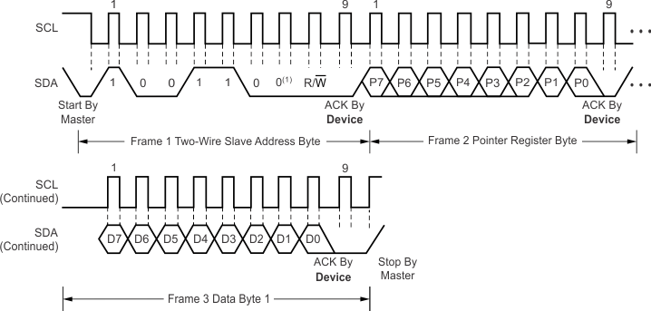
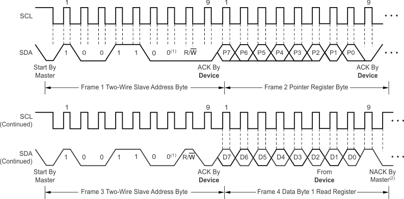
The TMP451-Q1 device is two-wire and SMBus-compatible. Figure 7-4 and Figure 7-5 show the timing for various operations on the TMP451-Q1 device. The bus definitions are as follows:
- Bus Idle:Both SDA and SCL lines remain high.
- Start Data Transfer:A change in the state of the SDA line, from high to low, while the SCL line is high, defines a start condition. Each data transfer initiates with a start condition.
- Stop Data Transfer:A change in the state of the SDA line from low to high while the SCL line is high defines a stop condition. Each data transfer terminates with a repeated start or stop condition.
- Data Transfer:The number of data bytes transferred between a start and a stop condition is not limited and is determined by the master device. The receiver acknowledges data transfer.
- Acknowledge:Each receiving device, when addressed, is obliged to generate an acknowledge bit. A device that acknowledges must pull down the SDA line during the acknowledge clock pulse in such a way that the SDA line is stable low during the high period of the acknowledge clock pulse. Take setup and hold times into account. On a master receive, data transfer termination can be signaled by the master generating a not-acknowledge on the last byte that has been transmitted by the slave.

Slave address 1001100 shown.
Figure 7-4 Two-Wire Timing Diagram for Write Word Format
Slave address 1001100 shown.
Master should leave SDA high to terminate a single-byte read operation.
Figure 7-5 Two-Wire Timing Diagram for Single-Byte Read Format