ZHCSCV4C October 2014 – April 2021 TMP451-Q1
PRODUCTION DATA
- 1 特性
- 2 应用
- 3 说明
- 4 Revision History
- 5 Pin Configuration and Functions
- 6 Specifications
-
7 Detailed Description
- 7.1 Overview
- 7.2 Functional Block Diagram
- 7.3 Feature Description
- 7.4 Device Functional Modes
- 7.5 Programming
- 7.6 Register Map
- 8 Application and Implementation
- 9 Power Supply Recommendations
- 10Layout
- 11Device and Documentation Support
- 12Mechanical, Packaging, and Orderable Information
7.3.4 Filtering
Remote junction temperature sensors are usually implemented in a noisy environment. Noise is most often created by fast digital signals, and it can corrupt measurements. The TMP451-Q1 device has a built-in, 65-kHz filter on the inputs of D+ and D– to minimize the effects of noise. However, a bypass capacitor placed differentially across the inputs of the remote temperature sensor is recommended to make the application more robust against unwanted coupled signals. For this capacitor, select a value of between 100 pF and 1 nF. Some applications attain better overall accuracy with additional series resistance; however, this increased accuracy is application-specific. When series resistance is added, the total value should not be greater than 1 kΩ. If filtering is required, suggested component values are 100 pF and 50 Ω on each input; exact values are application-specific.
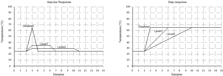
Additionally, a digital filter is available for the remote temperature measurements to further reduce the effect of noise. This filter is programmable and has two levels when enabled. Level 1 performs a moving average of four consecutive samples. Level 2 performs a moving average of eight consecutive samples. The value stored in the remote temperature result register is the output of the digital filter, and the ALERT and THERM limits are compared to it. This provides additional immunity to noise and spikes on the ALERT and THERM outputs. The filter responses are shown in Figure 7-1. The filter can be enabled or disabled by programming the desired levels in the digital filter register. The digital filter is disabled by default and on POR.
 Figure 7-1 Filter Response to Impulse and Step Inputs