ZHCSGB8C May 2017 – October 2019 TMP464
PRODUCTION DATA.
- 1 特性
- 2 应用
- 3 说明
- 4 修订历史记录
- 5 Pin Configuration and Functions
- 6 Specifications
-
7 Detailed Description
- 7.1 Overview
- 7.2 Functional Block Diagram
- 7.3 Feature Description
- 7.4 Device Functional Modes
- 7.5 Programming
- 7.6
Register Maps
- 7.6.1
Register Information
- 7.6.1.1 Pointer Register
- 7.6.1.2 Local and Remote Temperature Value Registers
- 7.6.1.3 Software Reset Register
- 7.6.1.4 THERM Status Register
- 7.6.1.5 THERM2 Status Register
- 7.6.1.6 Remote Channel Open Status Register
- 7.6.1.7 Configuration Register
- 7.6.1.8 η-Factor Correction Register
- 7.6.1.9 Remote Temperature Offset Register
- 7.6.1.10 THERM Hysteresis Register
- 7.6.1.11 Local and Remote THERM and THERM2 Limit Registers
- 7.6.1.12 Block Read - Auto Increment Pointer
- 7.6.1.13 Lock Register
- 7.6.1.14 Manufacturer and Device Identification Plus Revision Registers
- 7.6.1
Register Information
- 8 Application and Implementation
- 9 Power Supply Recommendations
- 10Layout
- 11器件和文档支持
- 12机械、封装和可订购信息
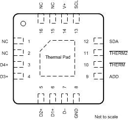
5 Pin Configuration and Functions
TMP464 RGT Package
16-Pin VQFN With Exposed Thermal Pad
Top View

NC - No internal connection
Pin Functions
| PIN | TYPE | DESCRIPTION | |
|---|---|---|---|
| NAME | NO. | ||
| ADD | 9 | Digital Input | Address select. Connect to GND, V+, SDA, or SCL. |
| D1+ | 6 | Analog input | Positive connection to remote temperature sensors. A total of 4 remote channels are supported. An unused channel must be connected to D–. |
| D2+ | 5 | Analog input | Positive connection to remote temperature sensors. A total of 4 remote channels are supported. An unused channel must be connected to D–. |
| D3+ | 4 | Analog input | Positive connection to remote temperature sensors. A total of 4 remote channels are supported. An unused channel must be connected to D–. |
| D4+ | 3 | Analog input | Positive connection to remote temperature sensors. A total of 4 remote channels are supported. An unused channel must be connected to D–. |
| D– | 7 | Analog input | Negative connection to remote temperature sensors. Common for 4 remote channels. |
| GND | 8 | Ground | Supply ground connection |
| NC | 1, 2, 15, 16 | — | No connection, may be left floating or connected to GND or V+ |
| SCL | 13 | Digital input | Serial clock line for I2C or SMBus compatible two-wire interface.
Input; requires a pullup resistor to a voltage between 1.7 V and 3.6 V (not necessarily V+) if driven by an open-drain output. |
| SDA | 12 | Bidirectional digital input-output | Serial data line for I2C- or SMBus compatible two-wire interface. Open-drain; requires a pullup resistor to a voltage between 1.7 V and 3.6 V, not necessarily V+. |
| THERM | 10 | Digital output | Thermal shutdown or fan-control pin.
Active low; open-drain; requires a pullup resistor to a voltage between 1.7 V and 3.6 V, not necessarily V+. If this pin is not used it may be left open or grounded. |
| THERM2 | 11 | Digital output | Second THERM output.
Active low; open-drain; requires a pullup resistor to a voltage between 1.7 V and 3.6 V, not necessarily V+. If this pin is not used it may be left open or grounded. |
| V+ | 14 | Power supply | Positive supply voltage, 1.7 V to 3.6 V; requires 0.1-µF bypass capacitor to ground. |