ZHCSFW9 December 2016 TMP708-Q1
PRODUCTION DATA.
6 Specifications
6.1 Absolute Maximum Ratings
over operating free-air temperature range (unless otherwise noted) (1)| MIN | MAX | UNIT | ||
|---|---|---|---|---|
| Voltage | Supply, VCC | –0.3 | 6 | V |
| Input, SET and HYST | –0.3 | VCC + 0.3 | ||
| Output, OT | –0.3 | 6 | ||
| Current | Input | 20 | mA | |
| Output | 20 | |||
| Temperature | Operating, TA | –40 | 125 | °C |
| Junction, TJ | 150 | |||
| Storatge, Tstg | –65 | 150 |
(1) Stresses beyond those listed under Absolute Maximum Ratings may cause permanent damage to the device. These are stress ratings only, which do not imply functional operation of the device at these or any other conditions beyond those indicated under Recommended Operating Conditions. Exposure to absolute-maximum-rated conditions for extended periods may affect device reliability.
6.2 ESD Ratings
| VALUE | UNIT | |||
|---|---|---|---|---|
| V(ESD) | Electrostatic discharge | Human-body model (HBM), per AEC Q100-002(1) | ±4000 | V |
| Charged-device model (CDM), per AEC Q100-011 | ±1000 | |||
(1) AEC Q100-002 indicates that HBM stressing shall be in accordance with the ANSI/ESDA/JEDEC JS-001 specification.
6.3 Recommended Operating Conditions
over operating free-air temperature range (unless otherwise noted)| MIN | NOM | MAX | UNIT | ||
|---|---|---|---|---|---|
| VCC | Supply voltage | 2.7 | 5.5 | V | |
| TA | Operating temperature | 0 | 125 | °C | |
6.4 Thermal Information
| THERMAL METRIC(1) | TMP708-Q1 | UNIT | |
|---|---|---|---|
| DBV (SOT-23) | |||
| 5 PINS | |||
| RθJA | Junction-to-ambient thermal resistance | 217.9 | °C/W |
| RθJC(top) | Junction-to-case (top) thermal resistance | 86.3 | °C/W |
| RθJB | Junction-to-board thermal resistance | 44.6 | °C/W |
| ψJT | Junction-to-top characterization parameter | 4.4 | °C/W |
| ψJB | Junction-to-board characterization parameter | 43.8 | °C/W |
| RθJC(bot) | Junction-to-case (bottom) thermal resistance | N/A | °C/W |
(1) For more information about traditional and new thermal metrics, see the Semiconductor and IC Package Thermal Metrics application report.
6.5 Electrical Characteristics
at TA = 0°C to 125°C and VCC = 2.7 V to 5.5 V (unless otherwise noted)| PARAMETER | TEST CONDITIONS | MIN | TYP | MAX | UNIT | |
|---|---|---|---|---|---|---|
| POWER SUPPLY | ||||||
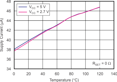
| ICC | Supply current | VCC = 5 V | 40 | 55 | µA | |
| VCC = 2.7 V | 40 | 55 | µA | |||
| TEMPERATURE | ||||||
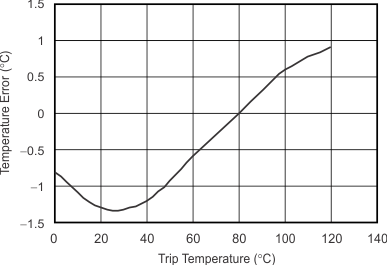
| TE | Temperature error | TA = 60°C to 100°C | ±0.5 | ±3.5 | °C | |
| DIGITAL INPUT (HYST) | ||||||
| VIH | High-level input voltage | 0.7 × VCC | V | |||
| VIL | Low-level input voltage | 0.3 × VCC | V | |||
| Ilkg_in | Input leakage current | 1 | µA | |||
| CIN | Input capacitance | 10 | pF | |||
| ANALOG INPUT (SET) | ||||||
| VIN | Input voltage range | 0 | VCC | V | ||
| DIGITAL OPEN-DRAIN OUTPUT (OT) | ||||||
| I(OT_SINK) | Output sink current | VOT = 0.3 V | 5 | 12 | mA | |
| Ilkg(OT) | Output leakage current | VOT = VCC | 1 | µA | ||
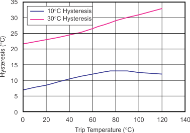
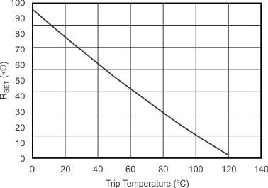
6.6 Typical Characteristics
at TA = 25°C and VCC = 2.7 V to 5.5 V (unless otherwise noted)


