ZHCSA18F March 2009 – February 2021 TMS320C28341 , TMS320C28342 , TMS320C28343 , TMS320C28343-Q1 , TMS320C28344 , TMS320C28345 , TMS320C28346 , TMS320C28346-Q1
PRODUCTION DATA
- 1 特性
- 2 应用
- 3 说明
- 4 Revision History
- 5 Device Comparison
- 6 Terminal Configuration and Functions
-
7 Specifications
- 7.1 Absolute Maximum Ratings (1) (1)
- 7.2 ESD Ratings – Automotive
- 7.3 ESD Ratings – Commercial
- 7.4 Recommended Operating Conditions
- 7.5 Power Consumption Summary
- 7.6 Electrical Characteristics
- 7.7 Thermal Resistance Characteristics
- 7.8 Thermal Design Considerations
- 7.9
Timing and Switching Characteristics
- 7.9.1 Timing Parameter Symbology
- 7.9.2 Power Sequencing
- 7.9.3 Clock Requirements and Characteristics
- 7.9.4
Peripherals
- 7.9.4.1
General-Purpose Input/Output (GPIO)
- 7.9.4.1.1 GPIO - Output Timing
- 7.9.4.1.2 GPIO - Input Timing
- 7.9.4.1.3 Sampling Window Width for Input Signals
- 7.9.4.1.4
Low-Power Mode Wakeup Timing
- 7.9.4.1.4.1 IDLE Mode Timing Requirements (1)
- 7.9.4.1.4.2 IDLE Mode Switching Characteristics (1)
- 7.9.4.1.4.3 IDLE Mode Timing Diagram
- 7.9.4.1.4.4 STANDBY Mode Timing Requirements
- 7.9.4.1.4.5 STANDBY Mode Switching Characteristics
- 7.9.4.1.4.6 STANDBY Mode Timing Diagram
- 7.9.4.1.4.7 HALT Mode Timing Requirements
- 7.9.4.1.4.8 HALT Mode Switching Characteristics
- 7.9.4.1.4.9 HALT Mode Timing Diagram
- 7.9.4.2 Enhanced Control Peripherals
- 7.9.4.3 External Interrupt Timing
- 7.9.4.4 I2C Electrical Specification and Timing
- 7.9.4.5 Serial Peripheral Interface (SPI) Timing
- 7.9.4.6
Multichannel Buffered Serial Port (McBSP) Timing
- 7.9.4.6.1 McBSP Transmit and Receive Timing
- 7.9.4.6.2
McBSP as SPI Master or Slave Timing
- 7.9.4.6.2.1 McBSP as SPI Master or Slave Timing Requirements (CLKSTP = 10b, CLKXP = 0) (1)
- 7.9.4.6.2.2 McBSP as SPI Master or Slave Switching Characteristics (CLKSTP = 10b, CLKXP = 0)
- 7.9.4.6.2.3 McBSP as SPI Master or Slave Timing Requirements (CLKSTP = 11b, CLKXP = 0) (1)
- 7.9.4.6.2.4 McBSP as SPI Master or Slave Switching Characteristics (CLKSTP = 11b, CLKXP = 0)
- 7.9.4.6.2.5 McBSP as SPI Master or Slave Timing Requirements (CLKSTP = 10b, CLKXP = 1) (1)
- 7.9.4.6.2.6 McBSP as SPI Master or Slave Switching Characteristics (CLKSTP = 10b, CLKXP = 1)
- 7.9.4.6.2.7 McBSP as SPI Master or Slave Timing Requirements (CLKSTP = 11b, CLKXP = 1) (1)
- 7.9.4.6.2.8 McBSP as SPI Master or Slave Switching Characteristics (CLKSTP = 11b, CLKXP = 1) (1)
- 7.9.4.1
General-Purpose Input/Output (GPIO)
- 7.9.5 Emulator Connection Without Signal Buffering for the MCU
- 7.9.6
External Interface (XINTF) Timing
- 7.9.6.1 USEREADY = 0
- 7.9.6.2 Synchronous Mode (USEREADY = 1, READYMODE = 0)
- 7.9.6.3 Asynchronous Mode (USEREADY = 1, READYMODE = 1)
- 7.9.6.4 XINTF Signal Alignment to XCLKOUT
- 7.9.6.5 External Interface Read Timing
- 7.9.6.6 External Interface Write Timing
- 7.9.6.7
External Interface Ready-on-Read Timing With One External Wait State
- 7.9.6.7.1 External Interface Read Switching Characteristics (Ready-on-Read, One Wait State)
- 7.9.6.7.2 External Interface Read Timing Requirements (Ready-on-Read, One Wait State)
- 7.9.6.7.3 Synchronous XREADY Timing Requirements (Ready-on-Read, One Wait State) (1)
- 7.9.6.7.4 Asynchronous XREADY Timing Requirements (Ready-on-Read, One Wait State)
- 7.9.6.8 External Interface Ready-on-Write Timing With One External Wait State
- 7.9.6.9 XHOLD and XHOLDA Timing
-
8 Detailed Description
- 8.1
Brief Descriptions
- 8.1.1 C28x CPU
- 8.1.2 Memory Bus (Harvard Bus Architecture)
- 8.1.3 Peripheral Bus
- 8.1.4 Real-Time JTAG and Analysis
- 8.1.5 External Interface (XINTF)
- 8.1.6 M0, M1 SARAMs
- 8.1.7 L0, L1, L2, L3, L4, L5, L6, L7, H0, H1, H2, H3, H4, H5 SARAMs
- 8.1.8 Boot ROM
- 8.1.9 Security
- 8.1.10 Peripheral Interrupt Expansion (PIE) Block
- 8.1.11 External Interrupts (XINT1–XINT7, XNMI)
- 8.1.12 Oscillator and PLL
- 8.1.13 Watchdog
- 8.1.14 Peripheral Clocking
- 8.1.15 Low-Power Modes
- 8.1.16 Peripheral Frames 0, 1, 2, 3 (PFn)
- 8.1.17 General-Purpose Input/Output (GPIO) Multiplexer
- 8.1.18 32-Bit CPU-Timers (0, 1, 2)
- 8.1.19 Control Peripherals
- 8.1.20 Serial Port Peripherals
- 8.2
Peripherals
- 8.2.1 DMA Overview
- 8.2.2 32-Bit CPU-Timer 0, CPU-Timer 1, CPU-Timer 2
- 8.2.3 Enhanced PWM Modules
- 8.2.4 High-Resolution PWM (HRPWM)
- 8.2.5 Enhanced CAP Modules
- 8.2.6 Enhanced QEP Modules
- 8.2.7 External ADC Interface
- 8.2.8 Multichannel Buffered Serial Port (McBSP) Module
- 8.2.9 Enhanced Controller Area Network (eCAN) Modules (eCAN-A and eCAN-B)
- 8.2.10 Serial Communications Interface (SCI) Modules (SCI-A, SCI-B, SCI-C)
- 8.2.11 Serial Peripheral Interface (SPI) Module (SPI-A, SPI-D)
- 8.2.12 Inter-Integrated Circuit (I2C)
- 8.2.13 GPIO MUX
- 8.2.14 External Interface (XINTF)
- 8.3 Memory Maps
- 8.4 Register Map
- 8.5 Interrupts
- 8.6 System Control
- 8.7 Low-Power Modes Block
- 8.1
Brief Descriptions
- 9 Applications, Implementation, and Layout
- 10Device and Documentation Support
- 11Mechanical, Packaging, and Orderable Information
8.3 Memory Maps
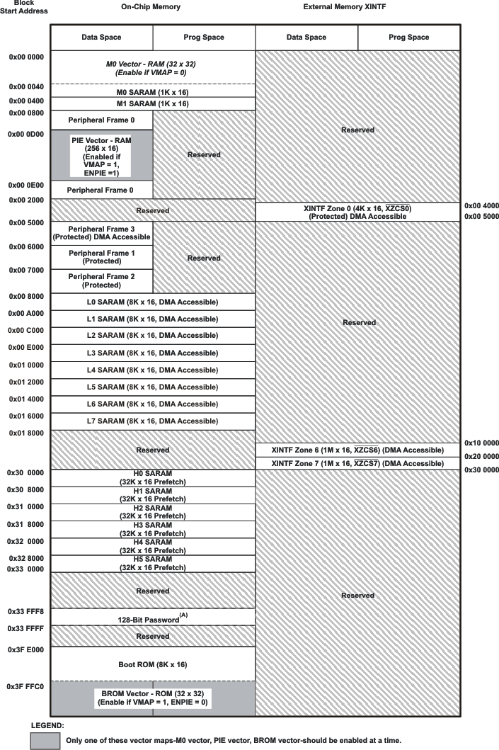
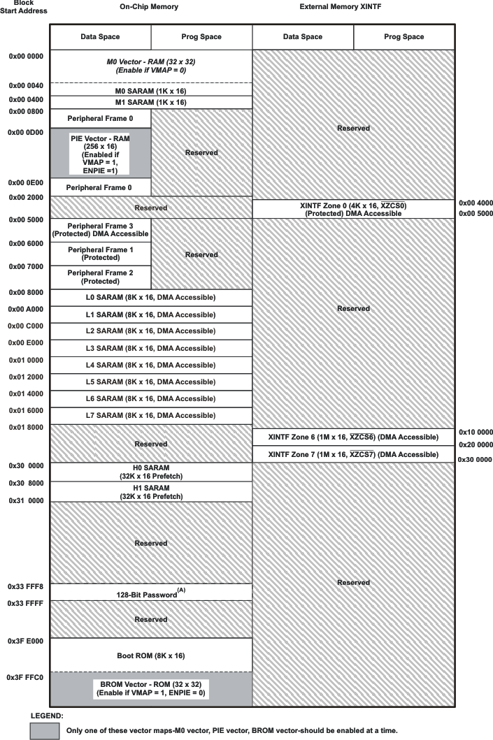
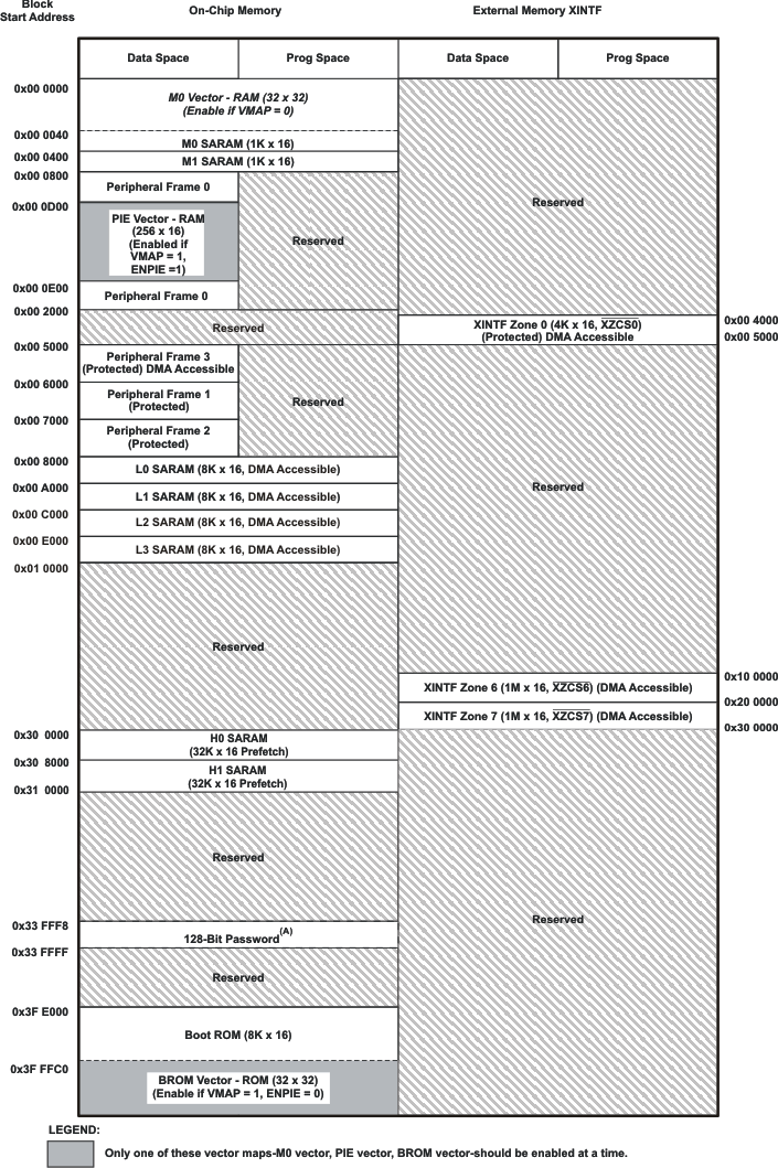
In Figure 8-21 to Figure 8-23, the following apply:
- Memory blocks are not to scale.
- Peripheral Frame 0, Peripheral Frame 1, Peripheral Frame 2, and Peripheral Frame 3 memory maps are restricted to data memory only. A user program cannot access these memory maps in program space.
- Protected means the order of "Write followed by Read" operations is preserved rather than the pipeline order. See the TMS320x2834x Delfino System Control and Interrupts Reference Guide for more details.
- Certain memory ranges are EALLOW protected against spurious writes after configuration.
- If the eCAN module is not used in an application, the RAM available (LAM, MOTS, MOTO, and mailbox RAM) can be used as general-purpose RAM. The CAN module clock should be enabled for this.


Peripheral Frame 1, Peripheral Frame 2, and Peripheral Frame 3 are grouped together to enable these blocks to be write/read peripheral block protected. The protected mode ensures that all accesses to these blocks happen as written. Because of the C28x pipeline, a write immediately followed by a read, to different memory locations, will appear in reverse order on the memory bus of the CPU. This can cause problems in certain peripheral applications where the user expected the write to occur first (as written). The C28x CPU supports a block protection mode where a region of memory can be protected so as to make sure that operations occur as written (the penalty is extra cycles are added to align the operations). This mode is programmable and by default, it will protect the selected zones.
The wait states for the various spaces in the memory map area are listed in Table 8-22.
| AREA | WAIT STATES (CPU) | WAIT STATES (DMA)(1) | COMMENTS |
|---|---|---|---|
| M0 and M1 SARAMs | 0-wait | No access | Fixed |
| Peripheral Frame 0 | 0-wait (writes) | No access (writes) | |
| 1-wait (reads) | 0-wait (reads) | ||
| Peripheral Frame 3 | 0-wait (writes) | 0-wait (writes) | Assumes no conflicts between CPU and DMA. |
| 2-wait (reads) | 1-wait (reads) | ||
| Peripheral Frame 1 | 0-wait (writes) | No access | Cycles can be extended by peripheral generated ready. |
| 2-wait (reads) | Consecutive writes to the CAN will experience a 1-cycle pipeline hit. | ||
| Peripheral Frame 2 | 0-wait (writes) | No access | Fixed. Cycles cannot be extended by the peripheral. |
| 2-wait (reads) | |||
| L0 SARAM | 0-wait data and program | Assumes no CPU conflicts | |
| L1 SARAM | |||
| L2 SARAM | |||
| L3 SARAM | |||
| L4 SARAM | 1-wait | Assumes no conflicts between CPU and DMA | |
| L5 SARAM | |||
| L6 SARAM | 1-wait | ||
| L7 SARAM | |||
| XINTF | Programmable | Programmed through the XTIMING registers or extendable through external XREADY signal. | |
| 1-wait minimum | 1-wait is minimum wait states allowed on external waveforms for both reads and writes on XINTF. | ||
| 0-wait minimum writes with write buffer enabled | 0-wait data (write) 0-wait data (read) | 0-wait minimum for writes assumes write buffer enabled and not full. Assumes no conflicts between CPU and DMA. When DMA and CPU try simultaneous conflict, 1-cycle delay is added for arbitration. | |
| H0 SARAM | 1-wait | No access | A program-access prefetch mechanism is enabled on these memories to improve instruction fetch performance for linear code execution. |
| H1 SARAM | |||
| H2 SARAM | |||
| H3 SARAM | |||
| H4 SARAM | |||
| H5 SARAM | |||
| Boot-ROM | 1-wait | No access |