ZHCSA18F March 2009 – February 2021 TMS320C28341 , TMS320C28342 , TMS320C28343 , TMS320C28343-Q1 , TMS320C28344 , TMS320C28345 , TMS320C28346 , TMS320C28346-Q1
PRODUCTION DATA
- 1 特性
- 2 应用
- 3 说明
- 4 Revision History
- 5 Device Comparison
- 6 Terminal Configuration and Functions
-
7 Specifications
- 7.1 Absolute Maximum Ratings (1) (1)
- 7.2 ESD Ratings – Automotive
- 7.3 ESD Ratings – Commercial
- 7.4 Recommended Operating Conditions
- 7.5 Power Consumption Summary
- 7.6 Electrical Characteristics
- 7.7 Thermal Resistance Characteristics
- 7.8 Thermal Design Considerations
- 7.9
Timing and Switching Characteristics
- 7.9.1 Timing Parameter Symbology
- 7.9.2 Power Sequencing
- 7.9.3 Clock Requirements and Characteristics
- 7.9.4
Peripherals
- 7.9.4.1
General-Purpose Input/Output (GPIO)
- 7.9.4.1.1 GPIO - Output Timing
- 7.9.4.1.2 GPIO - Input Timing
- 7.9.4.1.3 Sampling Window Width for Input Signals
- 7.9.4.1.4
Low-Power Mode Wakeup Timing
- 7.9.4.1.4.1 IDLE Mode Timing Requirements (1)
- 7.9.4.1.4.2 IDLE Mode Switching Characteristics (1)
- 7.9.4.1.4.3 IDLE Mode Timing Diagram
- 7.9.4.1.4.4 STANDBY Mode Timing Requirements
- 7.9.4.1.4.5 STANDBY Mode Switching Characteristics
- 7.9.4.1.4.6 STANDBY Mode Timing Diagram
- 7.9.4.1.4.7 HALT Mode Timing Requirements
- 7.9.4.1.4.8 HALT Mode Switching Characteristics
- 7.9.4.1.4.9 HALT Mode Timing Diagram
- 7.9.4.2 Enhanced Control Peripherals
- 7.9.4.3 External Interrupt Timing
- 7.9.4.4 I2C Electrical Specification and Timing
- 7.9.4.5 Serial Peripheral Interface (SPI) Timing
- 7.9.4.6
Multichannel Buffered Serial Port (McBSP) Timing
- 7.9.4.6.1 McBSP Transmit and Receive Timing
- 7.9.4.6.2
McBSP as SPI Master or Slave Timing
- 7.9.4.6.2.1 McBSP as SPI Master or Slave Timing Requirements (CLKSTP = 10b, CLKXP = 0) (1)
- 7.9.4.6.2.2 McBSP as SPI Master or Slave Switching Characteristics (CLKSTP = 10b, CLKXP = 0)
- 7.9.4.6.2.3 McBSP as SPI Master or Slave Timing Requirements (CLKSTP = 11b, CLKXP = 0) (1)
- 7.9.4.6.2.4 McBSP as SPI Master or Slave Switching Characteristics (CLKSTP = 11b, CLKXP = 0)
- 7.9.4.6.2.5 McBSP as SPI Master or Slave Timing Requirements (CLKSTP = 10b, CLKXP = 1) (1)
- 7.9.4.6.2.6 McBSP as SPI Master or Slave Switching Characteristics (CLKSTP = 10b, CLKXP = 1)
- 7.9.4.6.2.7 McBSP as SPI Master or Slave Timing Requirements (CLKSTP = 11b, CLKXP = 1) (1)
- 7.9.4.6.2.8 McBSP as SPI Master or Slave Switching Characteristics (CLKSTP = 11b, CLKXP = 1) (1)
- 7.9.4.1
General-Purpose Input/Output (GPIO)
- 7.9.5 Emulator Connection Without Signal Buffering for the MCU
- 7.9.6
External Interface (XINTF) Timing
- 7.9.6.1 USEREADY = 0
- 7.9.6.2 Synchronous Mode (USEREADY = 1, READYMODE = 0)
- 7.9.6.3 Asynchronous Mode (USEREADY = 1, READYMODE = 1)
- 7.9.6.4 XINTF Signal Alignment to XCLKOUT
- 7.9.6.5 External Interface Read Timing
- 7.9.6.6 External Interface Write Timing
- 7.9.6.7
External Interface Ready-on-Read Timing With One External Wait State
- 7.9.6.7.1 External Interface Read Switching Characteristics (Ready-on-Read, One Wait State)
- 7.9.6.7.2 External Interface Read Timing Requirements (Ready-on-Read, One Wait State)
- 7.9.6.7.3 Synchronous XREADY Timing Requirements (Ready-on-Read, One Wait State) (1)
- 7.9.6.7.4 Asynchronous XREADY Timing Requirements (Ready-on-Read, One Wait State)
- 7.9.6.8 External Interface Ready-on-Write Timing With One External Wait State
- 7.9.6.9 XHOLD and XHOLDA Timing
-
8 Detailed Description
- 8.1
Brief Descriptions
- 8.1.1 C28x CPU
- 8.1.2 Memory Bus (Harvard Bus Architecture)
- 8.1.3 Peripheral Bus
- 8.1.4 Real-Time JTAG and Analysis
- 8.1.5 External Interface (XINTF)
- 8.1.6 M0, M1 SARAMs
- 8.1.7 L0, L1, L2, L3, L4, L5, L6, L7, H0, H1, H2, H3, H4, H5 SARAMs
- 8.1.8 Boot ROM
- 8.1.9 Security
- 8.1.10 Peripheral Interrupt Expansion (PIE) Block
- 8.1.11 External Interrupts (XINT1–XINT7, XNMI)
- 8.1.12 Oscillator and PLL
- 8.1.13 Watchdog
- 8.1.14 Peripheral Clocking
- 8.1.15 Low-Power Modes
- 8.1.16 Peripheral Frames 0, 1, 2, 3 (PFn)
- 8.1.17 General-Purpose Input/Output (GPIO) Multiplexer
- 8.1.18 32-Bit CPU-Timers (0, 1, 2)
- 8.1.19 Control Peripherals
- 8.1.20 Serial Port Peripherals
- 8.2
Peripherals
- 8.2.1 DMA Overview
- 8.2.2 32-Bit CPU-Timer 0, CPU-Timer 1, CPU-Timer 2
- 8.2.3 Enhanced PWM Modules
- 8.2.4 High-Resolution PWM (HRPWM)
- 8.2.5 Enhanced CAP Modules
- 8.2.6 Enhanced QEP Modules
- 8.2.7 External ADC Interface
- 8.2.8 Multichannel Buffered Serial Port (McBSP) Module
- 8.2.9 Enhanced Controller Area Network (eCAN) Modules (eCAN-A and eCAN-B)
- 8.2.10 Serial Communications Interface (SCI) Modules (SCI-A, SCI-B, SCI-C)
- 8.2.11 Serial Peripheral Interface (SPI) Module (SPI-A, SPI-D)
- 8.2.12 Inter-Integrated Circuit (I2C)
- 8.2.13 GPIO MUX
- 8.2.14 External Interface (XINTF)
- 8.3 Memory Maps
- 8.4 Register Map
- 8.5 Interrupts
- 8.6 System Control
- 8.7 Low-Power Modes Block
- 8.1
Brief Descriptions
- 9 Applications, Implementation, and Layout
- 10Device and Documentation Support
- 11Mechanical, Packaging, and Orderable Information
8.2.14 External Interface (XINTF)
This section gives a top-level view of the external interface (XINTF) that is implemented on the C2834x devices.
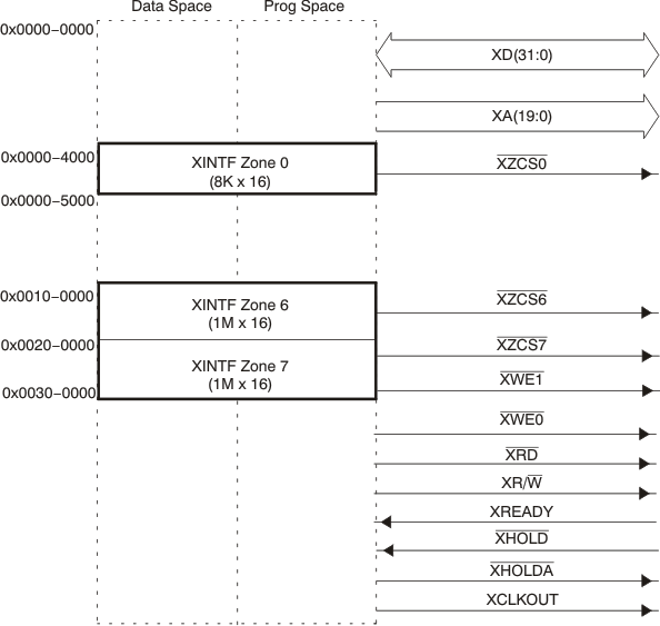
The XINTF is a nonmultiplexed asynchronous bus, similar to the 2812 XINTF. The XINTF is mapped into three fixed zones shown in Figure 8-18.
 Figure 8-18 External Interface Block Diagram
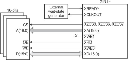
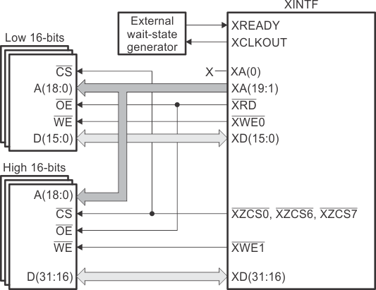
Figure 8-19 and Figure 8-20 show typical 16-bit and 32-bit data bus XINTF connections, illustrating how the functionality of the XA0 and XWE1 signals change, depending on the configuration. Table 8-21 defines XINTF configuration and control registers.
 Figure 8-19 Typical 16-Bit Data Bus XINTF Connections
 Figure 8-20 Typical 32-Bit Data Bus XINTF Connections
Table 8-21 XINTF Configuration and Control Register Mapping
| NAME | ADDRESS | SIZE (x16) | DESCRIPTION |
|---|---|---|---|
| XTIMING0 | 0x00−0B20 | 2 | XINTF Timing Register, Zone 0 |
| XTIMING6(1) | 0x00−0B2C | 2 | XINTF Timing Register, Zone 6 |
| XTIMING7 | 0x00−0B2E | 2 | XINTF Timing Register, Zone 7 |
| XINTCNF2(2) | 0x00−0B34 | 2 | XINTF Configuration Register |
| XBANK | 0x00−0B38 | 1 | XINTF Bank Control Register |
| XREVISION | 0x00−0B3A | 1 | XINTF Revision Register |
| XRESET | 0x00−0B3D | 1 | XINTF Reset Register |
(1) XTIMING1 - XTIMING5 are reserved for future expansion and are not currently used.
(2) XINTCNF1 is reserved and not currently used.