ZHCSGV6F June 2009 – January 2017 TMS320C6742
PRODUCTION DATA.
- 1器件概述
- 2Revision History
-
3Device Comparison
- 3.1 Device Characteristics
- 3.2 Device Compatibility
- 3.3 DSP Subsystem
- 3.4 Memory Map Summary
- 3.5 Pin Assignments
- 3.6 Pin Multiplexing Control
- 3.7
Terminal Functions
- 3.7.1 Device Reset, NMI and JTAG
- 3.7.2 High-Frequency Oscillator and PLL
- 3.7.3 Real-Time Clock and 32-kHz Oscillator
- 3.7.4 DEEPSLEEP Power Control
- 3.7.5 External Memory Interface A (EMIFA)
- 3.7.6 DDR2/mDDR Controller
- 3.7.7 Serial Peripheral Interface Modules (SPI)
- 3.7.8 Enhanced Capture/Auxiliary PWM Modules (eCAP0)
- 3.7.9 Enhanced Pulse Width Modulators (eHRPWM)
- 3.7.10 Boot
- 3.7.11 Universal Asynchronous Receiver/Transmitters (UART0)
- 3.7.12 Inter-Integrated Circuit Modules(I2C0)
- 3.7.13 Timers
- 3.7.14 Multichannel Audio Serial Ports (McASP)
- 3.7.15 Multichannel Buffered Serial Ports (McBSP)
- 3.7.16 Universal Host-Port Interface (UHPI)
- 3.7.17 General Purpose Input Output
- 3.7.18 Reserved and No Connect
- 3.7.19 Supply and Ground
- 3.8 Unused Pin Configurations
- 4Device Configuration
-
5Specifications
- 5.1 Absolute Maximum Ratings Over Operating Junction Temperature Range (Unless Otherwise Noted)
- 5.2 Handling Ratings
- 5.3 Recommended Operating Conditions
- 5.4 Notes on Recommended Power-On Hours (POH)
- 5.5 Electrical Characteristics Over Recommended Ranges of Supply Voltage and Operating Junction Temperature (Unless Otherwise Noted)
-
6Peripheral Information and Electrical Specifications
- 6.1 Parameter Information
- 6.2 Recommended Clock and Control Signal Transition Behavior
- 6.3 Power Supplies
- 6.4 Reset
- 6.5 Crystal Oscillator or External Clock Input
- 6.6 Clock PLLs
- 6.7 Interrupts
- 6.8 Power and Sleep Controller (PSC)
- 6.9 Enhanced Direct Memory Access Controller (EDMA3)
- 6.10 External Memory Interface A (EMIFA)
- 6.11
DDR2/mDDR Memory Controller
- 6.11.1 DDR2/mDDR Memory Controller Electrical Data/Timing
- 6.11.2 DDR2/mDDR Memory Controller Register Description(s)
- 6.11.3
DDR2/mDDR Interface
- 6.11.3.1 DDR2/mDDR Interface Schematic
- 6.11.3.2 Compatible JEDEC DDR2/mDDR Devices
- 6.11.3.3 PCB Stackup
- 6.11.3.4 Placement
- 6.11.3.5 DDR2/mDDR Keep Out Region
- 6.11.3.6 Bulk Bypass Capacitors
- 6.11.3.7 High-Speed Bypass Capacitors
- 6.11.3.8 Net Classes
- 6.11.3.9 DDR2/mDDR Signal Termination
- 6.11.3.10 VREF Routing
- 6.11.3.11 DDR2/mDDR CK and ADDR_CTRL Routing
- 6.11.3.12 DDR2/mDDR Boundary Scan Limitations
- 6.12 Memory Protection Units
- 6.13 Multichannel Audio Serial Port (McASP)
- 6.14
Multichannel Buffered Serial Port (McBSP)
- 6.14.1 McBSP Peripheral Register Description(s)
- 6.14.2
McBSP Electrical Data/Timing
- 6.14.2.1
Multichannel Buffered Serial Port (McBSP) Timing
- Table 6-47 Timing Requirements for McBSP1 [1.2V, 1.1V] (see )
- Table 6-48 Timing Requirements for McBSP1 [1.0V] (see )
- Table 6-49 Switching Characteristics for McBSP1 [1.2V, 1.1V] (see )
- Table 6-50 Switching Characteristics for McBSP1 [1.0V] (see )
- Table 6-51 Timing Requirements for McBSP1 FSR When GSYNC = 1 (see )
- 6.14.2.1
Multichannel Buffered Serial Port (McBSP) Timing
- 6.15 Serial Peripheral Interface Ports (SPI1)
- 6.16 Inter-Integrated Circuit Serial Ports (I2C)
- 6.17 Universal Asynchronous Receiver/Transmitter (UART)
- 6.18 Host-Port Interface (UHPI)
- 6.19 Enhanced Capture (eCAP) Peripheral
- 6.20 Enhanced High-Resolution Pulse-Width Modulator (eHRPWM)
- 6.21 Timers
- 6.22 Real Time Clock (RTC)
- 6.23 General-Purpose Input/Output (GPIO)
- 6.24 Emulation Logic
- 7Device and Documentation Support
- 8Mechanical Packaging and Orderable Information
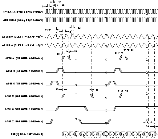
Table 6-45 Switching Characteristics for McASP0 (1.0V)(1)
| NO. | PARAMETER | 1.0V | UNIT | |||
|---|---|---|---|---|---|---|
| MIN | MAX | |||||
| 9 | tc(AHCLKRX) | Cycle time, AHCLKR/X | 35 | ns | ||
| 10 | tw(AHCLKRX) | Pulse duration, AHCLKR/X high or low | AH – 2.5(2) | ns | ||
| 11 | tc(ACLKRX) | Cycle time, ACLKR/X | ACLKR/X int | 35(4)(5) | ns | |
| 12 | tw(ACLKRX) | Pulse duration, ACLKR/X high or low | ACLKR/X int | A – 2.5(3) | ns | |
| 13 | td(ACLKRX-AFSRX) | Delay time, ACLKR/X transmit edge to AFSX/R output valid(6) | ACLKR/X int | -0.5 | 10 | ns |
| ACLKR/X ext input | 2 | 19 | ns | |||
| ACLKR/X ext output | 2 | 19 | ns | |||
| 14 | td(ACLKX-AXRV) | Delay time, ACLKX transmit edge to AXR output valid | ACLKR/X int | -0.5 | 10 | ns |
| ACLKR/X ext input | 2 | 19 | ns | |||
| ACLKR/X ext output | 2 | 19 | ns | |||
| 15 | tdis(ACLKX-AXRHZ) | Disable time, ACLKR/X transmit edge to AXR high impedance following last data bit | ACLKR/X int | 0 | 10 | ns |
| ACLKR/X ext | 2 | 19 | ns | |||
(1) McASP0 ACLKX0 internal – ACLKXCTL.CLKXM = 1, PDIR.ACLKX = 1
ACLKX0 external input – McASP0 ACLKXCTL.CLKXM = 0, PDIR.ACLKX = 0
ACLKX0 external output – McASP0ACLKXCTL.CLKXM = 0, PDIR.ACLKX = 1
ACLKR0 internal – McASP0 ACLKR0CTL.CLKRM = 1, PDIR.ACLKR =1
ACLKR0 external input – McASP0 ACLKRCTL.CLKRM = 0, PDIR.ACLKR = 0
ACLKR0 external output – McASP0 ACLKRCTL.CLKRM = 0, PDIR.ACLKR = 1
(2) AH = (AHCLKR/X period)/2 in ns. For example, when AHCLKR/X period is 25 ns, use AH = 12.5 ns.
(3) A = (ACLKR/X period)/2 in ns. For example, when AHCLKR/X period is 25 ns, use AH = 12.5 ns.
(4) P = SYSCLK2 period
(5) This timing is limited by the timing shown or 2P, whichever is greater.
(6) McASP0 ACLKXCTL.ASYNC=1: Receiver is clocked by its own ACLKR0

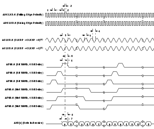
A. For CLKRP = CLKXP = 0, the McASP transmitter is configured for rising edge (to shift data out) and the McASP receiver is configured for falling edge (to shift data in).
B. For CLKRP = CLKXP = 1, the McASP transmitter is configured for falling edge (to shift data out) and the McASP receiver is configured for rising edge (to shift data in).
Figure 6-27 McASP Input Timings

A. For CLKRP = CLKXP = 1, the McASP transmitter is configured for falling edge (to shift data out) and the McASP receiver is configured for rising edge (to shift data in).
B. For CLKRP = CLKXP = 0, the McASP transmitter is configured for rising edge (to shift data out) and the McASP receiver is configured for falling edge (to shift data in).
Figure 6-28 McASP Output Timings