ZHCSGV6F June   2009  – January 2017 TMS320C6742

PRODUCTION DATA.  

  1. 1器件概述
    1. 1.1 特性
    2. 1.2 应用
    3. 1.3 说明
    4. 1.4 功能方框图
  2. 2Revision History
  3. 3Device Comparison
    1. 3.1 Device Characteristics
    2. 3.2 Device Compatibility
    3. 3.3 DSP Subsystem
      1. 3.3.1 C674x DSP CPU Description
      2. 3.3.2 DSP Memory Mapping
        1. 3.3.2.1 External Memories
        2. 3.3.2.2 DSP Internal Memories
        3. 3.3.2.3 C674x CPU
    4. 3.4 Memory Map Summary
      1. Table 3-4 C6742 Top Level Memory Map
    5. 3.5 Pin Assignments
      1. 3.5.1 Pin Map (Bottom View)
    6. 3.6 Pin Multiplexing Control
    7. 3.7 Terminal Functions
      1. 3.7.1  Device Reset, NMI and JTAG
      2. 3.7.2  High-Frequency Oscillator and PLL
      3. 3.7.3  Real-Time Clock and 32-kHz Oscillator
      4. 3.7.4  DEEPSLEEP Power Control
      5. 3.7.5  External Memory Interface A (EMIFA)
      6. 3.7.6  DDR2/mDDR Controller
      7. 3.7.7  Serial Peripheral Interface Modules (SPI)
      8. 3.7.8  Enhanced Capture/Auxiliary PWM Modules (eCAP0)
      9. 3.7.9  Enhanced Pulse Width Modulators (eHRPWM)
      10. 3.7.10 Boot
      11. 3.7.11 Universal Asynchronous Receiver/Transmitters (UART0)
      12. 3.7.12 Inter-Integrated Circuit Modules(I2C0)
      13. 3.7.13 Timers
      14. 3.7.14 Multichannel Audio Serial Ports (McASP)
      15. 3.7.15 Multichannel Buffered Serial Ports (McBSP)
      16. 3.7.16 Universal Host-Port Interface (UHPI)
      17. 3.7.17 General Purpose Input Output
      18. 3.7.18 Reserved and No Connect
      19. 3.7.19 Supply and Ground
    8. 3.8 Unused Pin Configurations
  4. 4Device Configuration
    1. 4.1 Boot Modes
    2. 4.2 SYSCFG Module
    3. 4.3 Pullup/Pulldown Resistors
  5. 5Specifications
    1. 5.1 Absolute Maximum Ratings Over Operating Junction Temperature Range (Unless Otherwise Noted)
    2. 5.2 Handling Ratings
    3. 5.3 Recommended Operating Conditions
    4. 5.4 Notes on Recommended Power-On Hours (POH)
    5. 5.5 Electrical Characteristics Over Recommended Ranges of Supply Voltage and Operating Junction Temperature (Unless Otherwise Noted)
  6. 6Peripheral Information and Electrical Specifications
    1. 6.1  Parameter Information
      1. 6.1.1 Parameter Information Device-Specific Information
        1. 6.1.1.1 Signal Transition Levels
    2. 6.2  Recommended Clock and Control Signal Transition Behavior
    3. 6.3  Power Supplies
      1. 6.3.1 Power-On Sequence
      2. 6.3.2 Power-Off Sequence
    4. 6.4  Reset
      1. 6.4.1 Power-On Reset (POR)
      2. 6.4.2 Warm Reset
      3. 6.4.3 Reset Electrical Data Timings
    5. 6.5  Crystal Oscillator or External Clock Input
    6. 6.6  Clock PLLs
      1. 6.6.1 PLL Device-Specific Information
      2. 6.6.2 Device Clock Generation
      3. 6.6.3 Dynamic Voltage and Frequency Scaling (DVFS)
    7. 6.7  Interrupts
      1. 6.7.1 DSP Interrupts
    8. 6.8  Power and Sleep Controller (PSC)
      1. 6.8.1 Power Domain and Module Topology
        1. 6.8.1.1 Power Domain States
        2. 6.8.1.2 Module States
    9. 6.9  Enhanced Direct Memory Access Controller (EDMA3)
      1. 6.9.1 EDMA3 Channel Synchronization Events
      2. 6.9.2 EDMA3 Peripheral Register Descriptions
    10. 6.10 External Memory Interface A (EMIFA)
      1. 6.10.1 EMIFA Asynchronous Memory Support
      2. 6.10.2 EMIFA Synchronous DRAM Memory Support
      3. 6.10.3 EMIFA SDRAM Loading Limitations
      4. 6.10.4 EMIFA Connection Examples
      5. 6.10.5 External Memory Interface Register Descriptions
      6. 6.10.6 EMIFA Electrical Data/Timing
        1. Table 6-19 Timing Requirements for EMIFA SDRAM Interface
        2. Table 6-20 Switching Characteristics for EMIFA SDRAM Interface
        3. Table 6-21 Timing Requirements for EMIFA Asynchronous Memory Interface
    11. 6.11 DDR2/mDDR Memory Controller
      1. 6.11.1 DDR2/mDDR Memory Controller Electrical Data/Timing
      2. 6.11.2 DDR2/mDDR Memory Controller Register Description(s)
      3. 6.11.3 DDR2/mDDR Interface
        1. 6.11.3.1  DDR2/mDDR Interface Schematic
        2. 6.11.3.2  Compatible JEDEC DDR2/mDDR Devices
        3. 6.11.3.3  PCB Stackup
        4. 6.11.3.4  Placement
        5. 6.11.3.5  DDR2/mDDR Keep Out Region
        6. 6.11.3.6  Bulk Bypass Capacitors
        7. 6.11.3.7  High-Speed Bypass Capacitors
        8. 6.11.3.8  Net Classes
        9. 6.11.3.9  DDR2/mDDR Signal Termination
        10. 6.11.3.10 VREF Routing
        11. 6.11.3.11 DDR2/mDDR CK and ADDR_CTRL Routing
        12. 6.11.3.12 DDR2/mDDR Boundary Scan Limitations
    12. 6.12 Memory Protection Units
    13. 6.13 Multichannel Audio Serial Port (McASP)
      1. 6.13.1 McASP Peripheral Registers Description(s)
      2. 6.13.2 McASP Electrical Data/Timing
        1. 6.13.2.1 Multichannel Audio Serial Port 0 (McASP0) Timing
          1. Table 6-42 Timing Requirements for McASP0 (1.2V, 1.1V)
          2. Table 6-43 Timing Requirements for McASP0 (1.0V)
          3. Table 6-44 Switching Characteristics for McASP0 (1.2V, 1.1V)
          4. Table 6-45 Switching Characteristics for McASP0 (1.0V)
    14. 6.14 Multichannel Buffered Serial Port (McBSP)
      1. 6.14.1 McBSP Peripheral Register Description(s)
      2. 6.14.2 McBSP Electrical Data/Timing
        1. 6.14.2.1 Multichannel Buffered Serial Port (McBSP) Timing
          1. Table 6-47 Timing Requirements for McBSP1 [1.2V, 1.1V] (see )
          2. Table 6-48 Timing Requirements for McBSP1 [1.0V] (see )
          3. Table 6-49 Switching Characteristics for McBSP1 [1.2V, 1.1V] (see )
          4. Table 6-50 Switching Characteristics for McBSP1 [1.0V] (see )
          5. Table 6-51 Timing Requirements for McBSP1 FSR When GSYNC = 1 (see )
    15. 6.15 Serial Peripheral Interface Ports (SPI1)
      1. 6.15.1 SPI Peripheral Registers Description(s)
      2. 6.15.2 SPI Electrical Data/Timing
        1. 6.15.2.1 Serial Peripheral Interface (SPI) Timing
          1. Table 6-53 General Timing Requirements for SPI1 Master Modes
          2. Table 6-54 General Timing Requirements for SPI1 Slave Modes
          3. Table 6-55 Additional SPI1 Master Timings, 4-Pin Enable Option
          4. Table 6-56 Additional SPI1 Master Timings, 4-Pin Chip Select Option
    16. 6.16 Inter-Integrated Circuit Serial Ports (I2C)
      1. 6.16.1 I2C Device-Specific Information
      2. 6.16.2 I2C Peripheral Registers Description(s)
      3. 6.16.3 I2C Electrical Data/Timing
        1. 6.16.3.1 Inter-Integrated Circuit (I2C) Timing
          1. Table 6-62 Timing Requirements for I2C Input
          2. Table 6-63 Switching Characteristics for I2C
    17. 6.17 Universal Asynchronous Receiver/Transmitter (UART)
      1. 6.17.1 UART Peripheral Registers Description(s)
      2. 6.17.2 UART Electrical Data/Timing
        1. Table 6-65 Timing Requirements for UART Receive (see )
        2. Table 6-66 Switching Characteristics Over Recommended Operating Conditions for UARTx Transmit (see )
    18. 6.18 Host-Port Interface (UHPI)
      1. 6.18.1 HPI Device-Specific Information
      2. 6.18.2 HPI Peripheral Register Description(s)
      3. 6.18.3 HPI Electrical Data/Timing
        1. Table 6-68 Timing Requirements for Host-Port Interface [1.2V, 1.1V]
        2. Table 6-69 Switching Characteristics Over Recommended Operating Conditions for Host-Port Interface [1.2V, 1.1V]
        3. Table 6-70 Switching Characteristics Over Recommended Operating Conditions for Host-Port Interface [1.0V]
    19. 6.19 Enhanced Capture (eCAP) Peripheral
      1. Table 6-72 Timing Requirements for Enhanced Capture (eCAP)
      2. Table 6-73 Switching Characteristics Over Recommended Operating Conditions for eCAP
    20. 6.20 Enhanced High-Resolution Pulse-Width Modulator (eHRPWM)
      1. 6.20.1 Enhanced Pulse Width Modulator (eHRPWM) Timing
        1. Table 6-75 Timing Requirements for eHRPWM
        2. Table 6-76 Switching Characteristics Over Recommended Operating Conditions for eHRPWM
      2. 6.20.2 Trip-Zone Input Timing
    21. 6.21 Timers
      1. 6.21.1 Timer Electrical Data/Timing
        1. Table 6-79 Timing Requirements for Timer Input (see )
        2. Table 6-80 Switching Characteristics Over Recommended Operating Conditions for Timer Output
    22. 6.22 Real Time Clock (RTC)
      1. 6.22.1 Clock Source
      2. 6.22.2 Real-Time Clock Register Descriptions
    23. 6.23 General-Purpose Input/Output (GPIO)
      1. 6.23.1 GPIO Register Description(s)
      2. 6.23.2 GPIO Peripheral Input/Output Electrical Data/Timing
        1. Table 6-83 Timing Requirements for GPIO Inputs (see )
        2. Table 6-84 Switching Characteristics Over Recommended Operating Conditions for GPIO Outputs (see )
      3. 6.23.3 GPIO Peripheral External Interrupts Electrical Data/Timing
        1. Table 6-85 Timing Requirements for External Interrupts (see )
    24. 6.24 Emulation Logic
      1. 6.24.1 JTAG Port Description
      2. 6.24.2 Scan Chain Configuration Parameters
      3. 6.24.3 Initial Scan Chain Configuration
      4. 6.24.4 IEEE 1149.1 JTAG
        1. 6.24.4.1 JTAG Peripheral Register Description(s) – JTAG ID Register (DEVIDR0)
        2. 6.24.4.2 JTAG Test-Port Electrical Data/Timing
          1. Table 6-91 Timing Requirements for JTAG Test Port (see )
          2. Table 6-92 Switching Characteristics Over Recommended Operating Conditions for JTAG Test Port (see )
      5. 6.24.5 JTAG 1149.1 Boundary Scan Considerations
  7. 7Device and Documentation Support
    1. 7.1 Device Nomenclature
    2. 7.2 Tools and Software
    3. 7.3 Documentation Support
    4. 7.4 社区资源
    5. 7.5 商标
    6. 7.6 静电放电警告
    7. 7.7 出口管制提示
    8. 7.8 术语表
  8. 8Mechanical Packaging and Orderable Information
    1. 8.1 Thermal Data for ZCE Package
    2. 8.2 Thermal Data for ZWT Package
    3. 8.3 Packaging Information

封装选项

请参考 PDF 数据表获取器件具体的封装图。

机械数据 (封装 | 引脚)
  • ZWT|361
散热焊盘机械数据 (封装 | 引脚)
订购信息

Device Nomenclature

To designate the stages in the product development cycle, TI assigns prefixes to the part numbers of all DSP devices and support tools. Each DSP commercial family member has one of three prefixes: TMX, TMP, or TMS (e.g., TMS320C6745). Texas Instruments recommends two of three possible prefix designators for its support tools: TMDX and TMDS. These prefixes represent evolutionary stages of product development from engineering prototypes (TMX/TMDX) through fully qualified production devices/tools (TMS/TMDS).

Device development evolutionary flow:

    TMX Experimental device that is not necessarily representative of the final device's electrical specifications.
    TMP Final silicon die that conforms to the device's electrical specifications but has not completed quality and reliability verification.
    TMS Fully-qualified production device.

Support tool development evolutionary flow:

    TMDX Development-support product that has not yet completed Texas Instruments internal qualification testing.
    TMDS Fully qualified development-support product.

TMX and TMP devices and TMDX development-support tools are shipped against the following disclaimer:

"Developmental product is intended for internal evaluation purposes."

TMS devices and TMDS development-support tools have been characterized fully, and the quality and reliability of the device have been demonstrated fully. TI's standard warranty applies.

Predictions show that prototype devices (TMX or TMP) have a greater failure rate than the standard production devices. Texas Instruments recommends that these devices not be used in any production system because their expected end-use failure rate still is undefined. Only qualified production devices are to be used.

TI device nomenclature also includes a suffix with the device family name. This suffix indicates the package type (for example, ZWT), the temperature range (for example, "Blank" is the commercial temperature range), and the device speed range in megahertz (for example, "Blank" is the default).

Figure 7-1 provides a legend for reading the complete device.
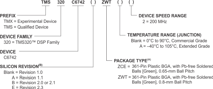
TMS320C6742 nomen_freon_c6742_prs587.gif
BGA = Ball Grid Array
Parts marked revision B are silicon revision 2.1 if '21' is marked on the package, and silicon revision 2.0 if there is no '21' marking.
Figure 7-1 Device Nomenclature