ZHCSGV6F June 2009 – January 2017 TMS320C6742
PRODUCTION DATA.
- 1器件概述
- 2Revision History
-
3Device Comparison
- 3.1 Device Characteristics
- 3.2 Device Compatibility
- 3.3 DSP Subsystem
- 3.4 Memory Map Summary
- 3.5 Pin Assignments
- 3.6 Pin Multiplexing Control
- 3.7
Terminal Functions
- 3.7.1 Device Reset, NMI and JTAG
- 3.7.2 High-Frequency Oscillator and PLL
- 3.7.3 Real-Time Clock and 32-kHz Oscillator
- 3.7.4 DEEPSLEEP Power Control
- 3.7.5 External Memory Interface A (EMIFA)
- 3.7.6 DDR2/mDDR Controller
- 3.7.7 Serial Peripheral Interface Modules (SPI)
- 3.7.8 Enhanced Capture/Auxiliary PWM Modules (eCAP0)
- 3.7.9 Enhanced Pulse Width Modulators (eHRPWM)
- 3.7.10 Boot
- 3.7.11 Universal Asynchronous Receiver/Transmitters (UART0)
- 3.7.12 Inter-Integrated Circuit Modules(I2C0)
- 3.7.13 Timers
- 3.7.14 Multichannel Audio Serial Ports (McASP)
- 3.7.15 Multichannel Buffered Serial Ports (McBSP)
- 3.7.16 Universal Host-Port Interface (UHPI)
- 3.7.17 General Purpose Input Output
- 3.7.18 Reserved and No Connect
- 3.7.19 Supply and Ground
- 3.8 Unused Pin Configurations
- 4Device Configuration
-
5Specifications
- 5.1 Absolute Maximum Ratings Over Operating Junction Temperature Range (Unless Otherwise Noted)
- 5.2 Handling Ratings
- 5.3 Recommended Operating Conditions
- 5.4 Notes on Recommended Power-On Hours (POH)
- 5.5 Electrical Characteristics Over Recommended Ranges of Supply Voltage and Operating Junction Temperature (Unless Otherwise Noted)
-
6Peripheral Information and Electrical Specifications
- 6.1 Parameter Information
- 6.2 Recommended Clock and Control Signal Transition Behavior
- 6.3 Power Supplies
- 6.4 Reset
- 6.5 Crystal Oscillator or External Clock Input
- 6.6 Clock PLLs
- 6.7 Interrupts
- 6.8 Power and Sleep Controller (PSC)
- 6.9 Enhanced Direct Memory Access Controller (EDMA3)
- 6.10 External Memory Interface A (EMIFA)
- 6.11
DDR2/mDDR Memory Controller
- 6.11.1 DDR2/mDDR Memory Controller Electrical Data/Timing
- 6.11.2 DDR2/mDDR Memory Controller Register Description(s)
- 6.11.3
DDR2/mDDR Interface
- 6.11.3.1 DDR2/mDDR Interface Schematic
- 6.11.3.2 Compatible JEDEC DDR2/mDDR Devices
- 6.11.3.3 PCB Stackup
- 6.11.3.4 Placement
- 6.11.3.5 DDR2/mDDR Keep Out Region
- 6.11.3.6 Bulk Bypass Capacitors
- 6.11.3.7 High-Speed Bypass Capacitors
- 6.11.3.8 Net Classes
- 6.11.3.9 DDR2/mDDR Signal Termination
- 6.11.3.10 VREF Routing
- 6.11.3.11 DDR2/mDDR CK and ADDR_CTRL Routing
- 6.11.3.12 DDR2/mDDR Boundary Scan Limitations
- 6.12 Memory Protection Units
- 6.13 Multichannel Audio Serial Port (McASP)
- 6.14
Multichannel Buffered Serial Port (McBSP)
- 6.14.1 McBSP Peripheral Register Description(s)
- 6.14.2
McBSP Electrical Data/Timing
- 6.14.2.1
Multichannel Buffered Serial Port (McBSP) Timing
- Table 6-47 Timing Requirements for McBSP1 [1.2V, 1.1V] (see )
- Table 6-48 Timing Requirements for McBSP1 [1.0V] (see )
- Table 6-49 Switching Characteristics for McBSP1 [1.2V, 1.1V] (see )
- Table 6-50 Switching Characteristics for McBSP1 [1.0V] (see )
- Table 6-51 Timing Requirements for McBSP1 FSR When GSYNC = 1 (see )
- 6.14.2.1
Multichannel Buffered Serial Port (McBSP) Timing
- 6.15 Serial Peripheral Interface Ports (SPI1)
- 6.16 Inter-Integrated Circuit Serial Ports (I2C)
- 6.17 Universal Asynchronous Receiver/Transmitter (UART)
- 6.18 Host-Port Interface (UHPI)
- 6.19 Enhanced Capture (eCAP) Peripheral
- 6.20 Enhanced High-Resolution Pulse-Width Modulator (eHRPWM)
- 6.21 Timers
- 6.22 Real Time Clock (RTC)
- 6.23 General-Purpose Input/Output (GPIO)
- 6.24 Emulation Logic
- 7Device and Documentation Support
- 8Mechanical Packaging and Orderable Information
6.5 Crystal Oscillator or External Clock Input
The device includes two choices to provide an external clock input, which is fed to the on-chip PLLs to generate
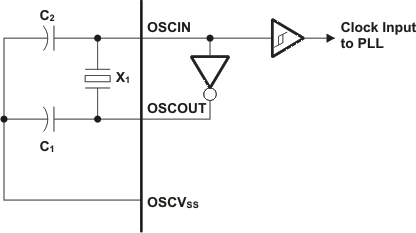
high-frequency system clocks. These options are illustrated in Figure 6-6 and Figure 6-7. For input clock frequencies between 12 and 20 MHz, a crystal with 80 ohm max ESR is recommended. For input clock frequencies between 20 and 30 MHz, a crystal with 60 ohm max ESR is recommended. Typical load capacitance values are 10-20 pF, where the load capacitance is the series combination of C1 and C2.
The CLKMODE bit in the PLLCTL register must be 0 to use the on-chip oscillator. If CLKMODE is set to 1, the internal oscillator is disabled.
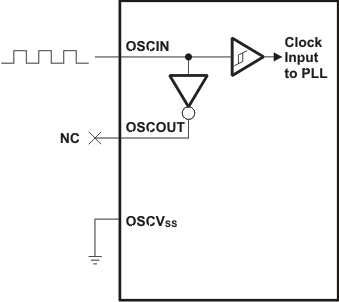
Figure 6-6 illustrates the option that uses on-chip 1.2V oscillator with external crystal circuit. Figure 6-7 illustrates the option that uses an external 1.2V clock input.
 Figure 6-6 On-Chip Oscillator
Table 6-2 Oscillator Timing Requirements
| PARAMETER | MIN | MAX | UNIT | |
|---|---|---|---|---|
| fosc | Oscillator frequency range (OSCIN/OSCOUT) | 12 | 30 | MHz |
 Figure 6-7 External 1.2V Clock Source
Table 6-3 OSCIN Timing Requirements for an Externally Driven Clock
| PARAMETER | MIN | MAX | UNIT | |
|---|---|---|---|---|
| fOSCIN | OSCIN frequency range | 12 | 50 | MHz |
| tc(OSCIN) | Cycle time, external clock driven on OSCIN | 20 | ns | |
| tw(OSCINH) | Pulse width high, external clock on OSCIN | 0.4 tc(OSCIN) | ns | |
| tw(OSCINL) | Pulse width low, external clock on OSCIN | 0.4 tc(OSCIN) | ns | |
| tt(OSCIN) | Transition time, OSCIN | 0.25P or 10 (1) | ns | |
| tj(OSCIN) | Period jitter, OSCIN | 0.02P | ns | |