SPRS565D April 2009 – June 2014 TMS320C6743
PRODUCTION DATA.
- 1TMS320C6743 Fixed- and Floating-Point Digital Signal Processor
- 2Revision History
-
3Device Overview
- 3.1 Device Characteristics
- 3.2 Device Compatibility
- 3.3 DSP Subsystem
- 3.4 Memory Map Summary
- 3.5 Pin Assignments
- 3.6
Terminal Functions
- 3.6.1 Device Reset and JTAG
- 3.6.2 High-Frequency Oscillator and PLL
- 3.6.3 External Memory Interface A (ASYNC)
- 3.6.4 External Memory Interface B (SDRAM only)
- 3.6.5 Serial Peripheral Interface Modules (SPI0)
- 3.6.6 Enhanced Capture/Auxiliary PWM Modules (eCAP0, eCAP1, eCAP2)
- 3.6.7 Enhanced Pulse Width Modulators (eHRPWM0, eHRPWM1, eHRPWM2)
- 3.6.8 Enhanced Quadrature Encoder Pulse Module (eQEP)
- 3.6.9 Boot
- 3.6.10 Universal Asynchronous Receiver/Transmitters (UART0, UART2)
- 3.6.11 Inter-Integrated Circuit Modules (I2C0, I2C1)
- 3.6.12 Timers
- 3.6.13 Multichannel Audio Serial Ports (McASP0, McASP1)
- 3.6.14 Ethernet Media Access Controller (EMAC)
- 3.6.15 Multimedia Card/Secure Digital (MMC/SD)
- 3.6.16 General-Purpose IO Only Terminal Functions
- 3.6.17 Reserved and No Connect Terminal Functions
- 3.6.18 Supply and Ground Terminal Functions
- 4Device Configuration
-
5Device Operating Conditions
- 5.1 Absolute Maximum Ratings Over Operating Junction Temperature Range (Unless Otherwise Noted)
- 5.2 Handling Ratings
- 5.3 Recommended Operating Conditions
- 5.4 Notes on Recommended Power-On Hours (POH)
- 5.5 Electrical Characteristics Over Recommended Ranges of Supply Voltage and Operating Junction Temperature (Unless Otherwise Noted)
-
6Peripheral Information and Electrical Specifications
- 6.1 Parameter Information
- 6.2 Recommended Clock and Control Signal Transition Behavior
- 6.3 Power Supplies
- 6.4 Reset
- 6.5 Crystal Oscillator or External Clock Input
- 6.6 Clock PLLs
- 6.7 DSP Interrupts
- 6.8 General-Purpose Input/Output (GPIO)
- 6.9 EDMA
- 6.10 External Memory Interface A (EMIFA)
- 6.11 External Memory Interface B (EMIFB)
- 6.12 Memory Protection Units
- 6.13 MMC / SD / SDIO (MMCSD)
- 6.14 Ethernet Media Access Controller (EMAC)
- 6.15 Management Data Input/Output (MDIO)
- 6.16 Multichannel Audio Serial Ports (McASP0, McASP1)
- 6.17
Serial Peripheral Interface Ports (SPI0)
- 6.17.1 SPI Peripheral Registers Description(s)
- 6.17.2
SPI Electrical Data/Timing
- 6.17.2.1
Serial Peripheral Interface (SPI) Timing
- Table 6-49 General Timing Requirements for SPI0 Master Modes
- Table 6-50 General Timing Requirements for SPI0 Slave Modes
- Table 6-51 Additional SPI0 Master Timings, 4-Pin Enable Option
- Table 6-52 Additional SPI0 Master Timings, 4-Pin Chip Select Option
- Table 6-53 Additional SPI0 Master Timings, 5-Pin Option
- Table 6-54 Additional SPI0 Slave Timings, 4-Pin Enable Option
- Table 6-55 Additional SPI0 Slave Timings, 4-Pin Chip Select Option
- Table 6-56 Additional SPI0 Slave Timings, 5-Pin Option
- 6.17.2.1
Serial Peripheral Interface (SPI) Timing
- 6.18 Enhanced Capture (eCAP) Peripheral
- 6.19 Enhanced Quadrature Encoder (eQEP) Peripheral
- 6.20 Enhanced Pulse Width Modulator (eHRPWM) Modules
- 6.21 Timers
- 6.22 Inter-Integrated Circuit Serial Ports (I2C0, I2C1)
- 6.23 Universal Asynchronous Receiver/Transmitter (UART)
- 6.24 Power and Sleep Controller (PSC)
- 6.25 Programmable Real-Time Unit Subsystem (PRUSS)
- 6.26 Emulation Logic
- 6.27 IEEE 1149.1 JTAG
- 7Device and Documentation Support
- 8Mechanical Packaging and Orderable Information
封装选项
请参考 PDF 数据表获取器件具体的封装图。
机械数据 (封装 | 引脚)
- ZKB|256
- PTP|176
散热焊盘机械数据 (封装 | 引脚)
- PTP|176
订购信息
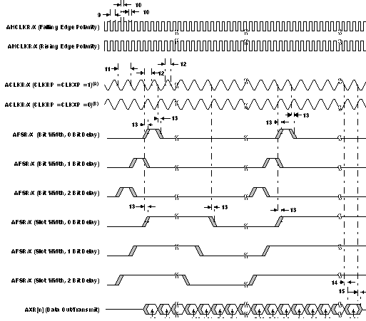
Table 6-47 McASP1 Switching Characteristics(1)
| NO. | PARAMETER | MIN | MAX | UNIT | |
|---|---|---|---|---|---|
| 9 | tc(AHCLKRX) | Cycle time, AHCLKR1 internal, AHCLKR1 output | 25 | ns | |
| Cycle time, AHCLKR1 external, AHCLKR1 output | 25 | ||||
| Cycle time, AHCLKX1 internal, AHCLKX1 output | 25 | ||||
| Cycle time, AHCLKX1 external, AHCLKX1 output | 25 | ||||
| 10 | tw(AHCLKRX) | Pulse duration, AHCLKR1 internal, AHCLKR1 output | (AHR/2) – 2.5(2) | ns | |
| Pulse duration, AHCLKR1 external, AHCLKR1 output | (AHR/2) – 2.5(2) | ||||
| Pulse duration, AHCLKX1 internal, AHCLKX1 output | (AHX/2) – 2.5(3) | ||||
| Pulse duration, AHCLKX1 external, AHCLKX1 output | (AHX/2) – 2.5(3) | ||||
| 11 | tc(ACLKRX) | Cycle time, ACLKR1 internal, ACLKR1 output | greater of 2P or 25(4) | ns | |
| Cycle time, ACLKR1 external, ACLKR1 output | greater of 2P or 25(4) | ||||
| Cycle time, ACLKX1 internal, ACLKX1 output | greater of 2P or 25(4) | ||||
| Cycle time, ACLKX1 external, ACLKX1 output | greater of 2P or 25(4) | ||||
| 12 | tw(ACLKRX) | Pulse duration, ACLKR1 internal, ACLKR1 output | (AR/2) – 2.5(5) | ns | |
| Pulse duration, ACLKR1 external, ACLKR1 output | (AR/2) – 2.5(5) | ||||
| Pulse duration, ACLKX1 internal, ACLKX1 output | (AX/2) – 2.5(6) | ||||
| Pulse duration, ACLKX1 external, ACLKX1 output | (AX/2) – 2.5(6) | ||||
| 13 | td(ACLKRX-AFSRX) | Delay time, ACLKR1 internal, AFSR output(7) | 0.5 | 6.7 | ns |
| Delay time, ACLKX1 internal, AFSX output | 0.5 | 6.7 | |||
| Delay time, ACLKR1 external input, AFSR output(7) | 3.4 | 13.8 | |||
| Delay time, ACLKX1 external input, AFSX output | 3.4 | 13.8 | |||
| Delay time, ACLKR1 external output, AFSR output(7) | 3.4 | 13.8 | |||
| Delay time, ACLKX1 external output, AFSX output | 3.4 | 13.8 | |||
| 14 | td(ACLKX-AXRV) | Delay time, ACLKX1 internal, AXR1[n] output | 0.5 | 6.7 | ns |
| Delay time, ACLKX1 external input, AXR1[n] output | 3.4 | 13.8 | |||
| Delay time, ACLKX1 external output, AXR1[n] output | 3.4 | 13.8 | |||
| 15 | tdis(ACLKX-AXRHZ) | Disable time, ACLKX1 internal, AXR1[n] output | 0.5 | 6.7 | ns |
| Disable time, ACLKX1 external input, AXR1[n] output | 3.9 | 13.8 | |||
| Disable time, ACLKX1 external output, AXR1[n] output | 3.9 | 13.8 | |||
(1) McASP1 ACLKX1 internal – ACLKXCTL.CLKXM = 1, PDIR.ACLKX = 1
McASP1 ACLKX1 external input – ACLKXCTL.CLKXM = 0, PDIR.ACLKX = 0
McASP1 ACLKX1 external output – ACLKXCTL.CLKXM = 0, PDIR.ACLKX = 1
McASP1 ACLKR1 internal – ACLKR1CTL.CLKRM = 1, PDIR.ACLKR =1
McASP1 ACLKR1 external input – ACLKRCTL.CLKRM = 0, PDIR.ACLKR = 0
McASP1 ACLKR1 external output – ACLKRCTL.CLKRM = 0, PDIR.ACLKR = 1
(2) AHR - Cycle time, AHCLKR1.
(3) AHX - Cycle time, AHCLKX1.
(4) P = SYSCLK2 period
(5) AR - ACLKR1 period.
(6) AX - ACLKX1 period.
(7) McASP1 ACLKXCTL.ASYNC=1: Receiver is clocked by its own ACLKR1

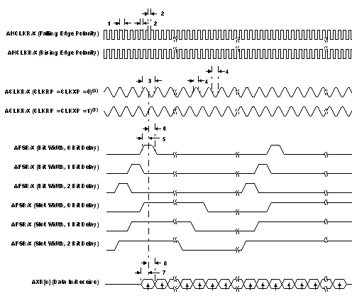
A. For CLKRP = CLKXP = 0, the McASP transmitter is configured for rising edge (to shift data out) and the McASP receiver is configured for falling edge (to shift data in).
B. For CLKRP = CLKXP = 1, the McASP transmitter is configured for falling edge (to shift data out) and the McASP receiver is configured for rising edge (to shift data in).
Figure 6-29 McASP Input Timings 
A. For CLKRP = CLKXP = 1, the McASP transmitter is configured for falling edge (to shift data out) and the McASP receiver is configured for rising edge (to shift data in).
B. For CLKRP = CLKXP = 0, the McASP transmitter is configured for rising edge (to shift data out) and the McASP receiver is configured for falling edge (to shift data in).
Figure 6-30 McASP Output Timings