ZHCS898O October 2003 – March 2019 TMS320F2801 , TMS320F28015 , TMS320F28016 , TMS320F2802 , TMS320F2806 , TMS320F2808 , TMS320F2809
PRODUCTION DATA.
- 1器件概述
- 2修订历史记录
- 3Device Comparison
- 4Terminal Configuration and Functions
-
5Specifications
- 5.1 Absolute Maximum Ratings
- 5.2 ESD Ratings – Automotive
- 5.3 ESD Ratings – Commercial
- 5.4 Recommended Operating Conditions
- 5.5
Power Consumption Summary
- Table 5-1 TMS320F2809, TMS320F2808 Current Consumption by Power-Supply Pins at 100-MHz SYSCLKOUT
- Table 5-2 TMS320F2806 Current Consumption by Power-Supply Pins at 100-MHz SYSCLKOUT
- Table 5-3 TMS320F2802, TMS320F2801 Current Consumption by Power-Supply Pins at 100-MHz SYSCLKOUT
- Table 5-4 TMS320C2802, TMS320C2801 Current Consumption by Power-Supply Pins at 100-MHz SYSCLKOUT
- 5.5.1 Reducing Current Consumption
- 5.5.2 Current Consumption Graphs
- 5.6 Electrical Characteristics
- 5.7 Thermal Resistance Characteristics for F280x 100-Ball GGM Package
- 5.8 Thermal Resistance Characteristics for F280x 100-Pin PZ Package
- 5.9 Thermal Resistance Characteristics for C280x 100-Ball GGM Package
- 5.10 Thermal Resistance Characteristics for C280x 100-Pin PZ Package
- 5.11 Thermal Resistance Characteristics for F2809 100-Ball GGM Package
- 5.12 Thermal Resistance Characteristics for F2809 100-Pin PZ Package
- 5.13 Thermal Design Considerations
- 5.14
Timing and Switching Characteristics
- 5.14.1 Timing Parameter Symbology
- 5.14.2 Power Sequencing
- 5.14.3 Clock Requirements and Characteristics
- 5.14.4
Peripherals
- 5.14.4.1 General-Purpose Input/Output (GPIO)
- 5.14.4.2 Enhanced Control Peripherals
- 5.14.4.3 External Interrupt Timing
- 5.14.4.4 I2C Electrical Specification and Timing
- 5.14.4.5 Serial Peripheral Interface (SPI) Timing
- 5.14.5 Emulator Connection Without Signal Buffering for the DSP
- 5.14.6 Flash Timing
- 5.15 On-Chip Analog-to-Digital Converter
- 5.16 Migrating From F280x Devices to C280x Devices
- 5.17 ROM Timing (C280x only)
-
6Detailed Description
- 6.1
Brief Descriptions
- 6.1.1 C28x CPU
- 6.1.2 Memory Bus (Harvard Bus Architecture)
- 6.1.3 Peripheral Bus
- 6.1.4 Real-Time JTAG and Analysis
- 6.1.5 Flash
- 6.1.6 ROM
- 6.1.7 M0, M1 SARAMs
- 6.1.8 L0, L1, H0 SARAMs
- 6.1.9 Boot ROM
- 6.1.10 Security
- 6.1.11 Peripheral Interrupt Expansion (PIE) Block
- 6.1.12 External Interrupts (XINT1, XINT2, XNMI)
- 6.1.13 Oscillator and PLL
- 6.1.14 Watchdog
- 6.1.15 Peripheral Clocking
- 6.1.16 Low-Power Modes
- 6.1.17 Peripheral Frames 0, 1, 2 (PFn)
- 6.1.18 General-Purpose Input/Output (GPIO) Multiplexer
- 6.1.19 32-Bit CPU-Timers (0, 1, 2)
- 6.1.20 Control Peripherals
- 6.1.21 Serial Port Peripherals
- 6.2
Peripherals
- 6.2.1 32-Bit CPU-Timers 0/1/2
- 6.2.2 Enhanced PWM Modules (ePWM1/2/3/4/5/6)
- 6.2.3 Hi-Resolution PWM (HRPWM)
- 6.2.4 Enhanced CAP Modules (eCAP1/2/3/4)
- 6.2.5 Enhanced QEP Modules (eQEP1/2)
- 6.2.6 Enhanced Analog-to-Digital Converter (ADC) Module
- 6.2.7 Enhanced Controller Area Network (eCAN) Modules (eCAN-A and eCAN-B)
- 6.2.8 Serial Communications Interface (SCI) Modules (SCI-A, SCI-B)
- 6.2.9 Serial Peripheral Interface (SPI) Modules (SPI-A, SPI-B, SPI-C, SPI-D)
- 6.2.10 Inter-Integrated Circuit (I2C)
- 6.2.11 GPIO MUX
- 6.3 Memory Maps
- 6.4 Register Map
- 6.5 Interrupts
- 6.6 System Control
- 6.7 Low-Power Modes Block
- 6.1
Brief Descriptions
- 7Applications, Implementation, and Layout
- 8器件和文档支持
- 9机械、封装和可订购信息
封装选项
请参考 PDF 数据表获取器件具体的封装图。
机械数据 (封装 | 引脚)
- PZ|100
- NMF|100
散热焊盘机械数据 (封装 | 引脚)
- PZ|100
订购信息
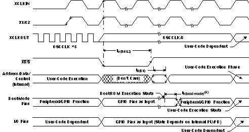
Table 5-8 Reset (XRS) Timing Requirements
| MIN | NOM | MAX | UNIT | ||||
|---|---|---|---|---|---|---|---|
| tw(RSL1)(1) | Pulse duration, stable XCLKIN to XRS high | 8tc(OSCCLK) | cycles | ||||
| tw(RSL2) | Pulse duration, XRS low | Warm reset | 8tc(OSCCLK) | cycles | |||
| tw(WDRS) | Pulse duration, reset pulse generated by watchdog | 512tc(OSCCLK) | cycles | ||||
| td(EX) | Delay time, address/data valid after XRS high | 32tc(OSCCLK) | cycles | ||||
| tOSCST(2) | Oscillator start-up time | 1 | 10 | ms | |||
| th(boot-mode) | Hold time for boot-mode pins | 200tc(OSCCLK) | cycles | ||||
(1) In addition to the tw(RSL1) requirement, XRS has to be low at least for 1 ms after VDD reaches 1.5 V.
(2) Dependent on crystal/resonator and board design.

A. After reset, the Boot ROM code samples BOOT Mode pins. Based on the status of the Boot Mode pin, the boot code branches to destination memory or boot code function. If Boot ROM code executes after power-on conditions (in debugger environment), the Boot code execution time is based on the current SYSCLKOUT speed. The SYSCLKOUT will be based on user environment and could be with or without PLL enabled.
Figure 5-7 Warm Reset Figure 5-8 shows an example for the effect of writing into PLLCR register. In the first phase, PLLCR = 0x0004 and SYSCLKOUT = OSCCLK x 2. The PLLCR is then written with 0x0008. Right after the PLLCR register is written, the PLL lock-up phase begins. During this phase, SYSCLKOUT = OSCCLK/2. After the PLL lock-up is complete (which takes 131072 OSCCLK cycles), SYSCLKOUT reflects the new operating frequency, OSCCLK x 4.
 Figure 5-8 Example of Effect of Writing Into PLLCR Register