ZHCS898O October 2003 – March 2019 TMS320F2801 , TMS320F28015 , TMS320F28016 , TMS320F2802 , TMS320F2806 , TMS320F2808 , TMS320F2809
PRODUCTION DATA.
- 1器件概述
- 2修订历史记录
- 3Device Comparison
- 4Terminal Configuration and Functions
-
5Specifications
- 5.1 Absolute Maximum Ratings
- 5.2 ESD Ratings – Automotive
- 5.3 ESD Ratings – Commercial
- 5.4 Recommended Operating Conditions
- 5.5
Power Consumption Summary
- Table 5-1 TMS320F2809, TMS320F2808 Current Consumption by Power-Supply Pins at 100-MHz SYSCLKOUT
- Table 5-2 TMS320F2806 Current Consumption by Power-Supply Pins at 100-MHz SYSCLKOUT
- Table 5-3 TMS320F2802, TMS320F2801 Current Consumption by Power-Supply Pins at 100-MHz SYSCLKOUT
- Table 5-4 TMS320C2802, TMS320C2801 Current Consumption by Power-Supply Pins at 100-MHz SYSCLKOUT
- 5.5.1 Reducing Current Consumption
- 5.5.2 Current Consumption Graphs
- 5.6 Electrical Characteristics
- 5.7 Thermal Resistance Characteristics for F280x 100-Ball GGM Package
- 5.8 Thermal Resistance Characteristics for F280x 100-Pin PZ Package
- 5.9 Thermal Resistance Characteristics for C280x 100-Ball GGM Package
- 5.10 Thermal Resistance Characteristics for C280x 100-Pin PZ Package
- 5.11 Thermal Resistance Characteristics for F2809 100-Ball GGM Package
- 5.12 Thermal Resistance Characteristics for F2809 100-Pin PZ Package
- 5.13 Thermal Design Considerations
- 5.14
Timing and Switching Characteristics
- 5.14.1 Timing Parameter Symbology
- 5.14.2 Power Sequencing
- 5.14.3 Clock Requirements and Characteristics
- 5.14.4
Peripherals
- 5.14.4.1 General-Purpose Input/Output (GPIO)
- 5.14.4.2 Enhanced Control Peripherals
- 5.14.4.3 External Interrupt Timing
- 5.14.4.4 I2C Electrical Specification and Timing
- 5.14.4.5 Serial Peripheral Interface (SPI) Timing
- 5.14.5 Emulator Connection Without Signal Buffering for the DSP
- 5.14.6 Flash Timing
- 5.15 On-Chip Analog-to-Digital Converter
- 5.16 Migrating From F280x Devices to C280x Devices
- 5.17 ROM Timing (C280x only)
-
6Detailed Description
- 6.1
Brief Descriptions
- 6.1.1 C28x CPU
- 6.1.2 Memory Bus (Harvard Bus Architecture)
- 6.1.3 Peripheral Bus
- 6.1.4 Real-Time JTAG and Analysis
- 6.1.5 Flash
- 6.1.6 ROM
- 6.1.7 M0, M1 SARAMs
- 6.1.8 L0, L1, H0 SARAMs
- 6.1.9 Boot ROM
- 6.1.10 Security
- 6.1.11 Peripheral Interrupt Expansion (PIE) Block
- 6.1.12 External Interrupts (XINT1, XINT2, XNMI)
- 6.1.13 Oscillator and PLL
- 6.1.14 Watchdog
- 6.1.15 Peripheral Clocking
- 6.1.16 Low-Power Modes
- 6.1.17 Peripheral Frames 0, 1, 2 (PFn)
- 6.1.18 General-Purpose Input/Output (GPIO) Multiplexer
- 6.1.19 32-Bit CPU-Timers (0, 1, 2)
- 6.1.20 Control Peripherals
- 6.1.21 Serial Port Peripherals
- 6.2
Peripherals
- 6.2.1 32-Bit CPU-Timers 0/1/2
- 6.2.2 Enhanced PWM Modules (ePWM1/2/3/4/5/6)
- 6.2.3 Hi-Resolution PWM (HRPWM)
- 6.2.4 Enhanced CAP Modules (eCAP1/2/3/4)
- 6.2.5 Enhanced QEP Modules (eQEP1/2)
- 6.2.6 Enhanced Analog-to-Digital Converter (ADC) Module
- 6.2.7 Enhanced Controller Area Network (eCAN) Modules (eCAN-A and eCAN-B)
- 6.2.8 Serial Communications Interface (SCI) Modules (SCI-A, SCI-B)
- 6.2.9 Serial Peripheral Interface (SPI) Modules (SPI-A, SPI-B, SPI-C, SPI-D)
- 6.2.10 Inter-Integrated Circuit (I2C)
- 6.2.11 GPIO MUX
- 6.3 Memory Maps
- 6.4 Register Map
- 6.5 Interrupts
- 6.6 System Control
- 6.7 Low-Power Modes Block
- 6.1
Brief Descriptions
- 7Applications, Implementation, and Layout
- 8器件和文档支持
- 9机械、封装和可订购信息
封装选项
请参考 PDF 数据表获取器件具体的封装图。
机械数据 (封装 | 引脚)
- PZ|100
- NMF|100
散热焊盘机械数据 (封装 | 引脚)
- PZ|100
订购信息
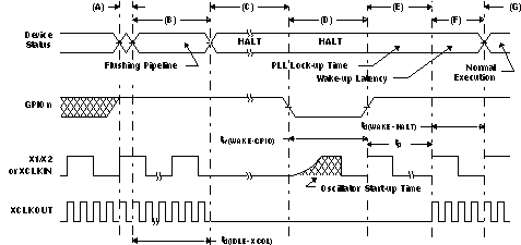
Table 5-20 HALT Mode Switching Characteristics
| PARAMETER | MIN | MAX | UNIT | |
|---|---|---|---|---|
| td(IDLE-XCOL) | Delay time, IDLE instruction executed to XCLKOUT low | 32tc(SCO) | 45tc(SCO) | cycles |
| tp | PLL lock-up time | 131072tc(OSCCLK) | cycles | |
| td(WAKE-HALT) | Delay time, PLL lock to program execution resume
|
1125tc(SCO) | cycles | |
|
35tc(SCO) | cycles | ||

A. IDLE instruction is executed to put the device into HALT mode.
B. The PLL block responds to the HALT signal. SYSCLKOUT is held for approximately 32 cycles (if CLKINDIV = 0) or 64 cycles (if CLKINDIV = 1) before the oscillator is turned off and the CLKIN to the core is stopped. This delay enables the CPU pipe and any other pending operations to flush properly.
C. Clocks to the peripherals are turned off and the PLL is shut down. If a quartz crystal or ceramic resonator is used as the clock source, the internal oscillator is shut down as well. The device is now in HALT mode and consumes absolute minimum power.
D. When the GPIOn pin (used to bring the device out of HALT) is driven low, the oscillator is turned on and the oscillator wake-up sequence is initiated. The GPIO pin should be driven high only after the oscillator has stabilized. This enables the provision of a clean clock signal during the PLL lock sequence. Since the falling edge of the GPIO pin asynchronously begins the wakeup process, care should be taken to maintain a low noise environment prior to entering and during HALT mode.
E. Once the oscillator has stabilized, the PLL lock sequence is initiated, which takes 131,072 OSCCLK (X1/X2 or X1 or XCLKIN) cycles. Note that these 131,072 clock cycles are applicable even when the PLL is disabled (that is, code execution will be delayed by this duration even when the PLL is disabled).
F. Clocks to the core and peripherals are enabled. The HALT mode is now exited. The device will respond to the interrupt (if enabled), after a latency.
G. Normal operation resumes.
Figure 5-15 HALT Wake-Up Using GPIOn