ZHCS898O October 2003 – March 2019 TMS320F2801 , TMS320F28015 , TMS320F28016 , TMS320F2802 , TMS320F2806 , TMS320F2808 , TMS320F2809
PRODUCTION DATA.
- 1器件概述
- 2修订历史记录
- 3Device Comparison
- 4Terminal Configuration and Functions
-
5Specifications
- 5.1 Absolute Maximum Ratings
- 5.2 ESD Ratings – Automotive
- 5.3 ESD Ratings – Commercial
- 5.4 Recommended Operating Conditions
- 5.5
Power Consumption Summary
- Table 5-1 TMS320F2809, TMS320F2808 Current Consumption by Power-Supply Pins at 100-MHz SYSCLKOUT
- Table 5-2 TMS320F2806 Current Consumption by Power-Supply Pins at 100-MHz SYSCLKOUT
- Table 5-3 TMS320F2802, TMS320F2801 Current Consumption by Power-Supply Pins at 100-MHz SYSCLKOUT
- Table 5-4 TMS320C2802, TMS320C2801 Current Consumption by Power-Supply Pins at 100-MHz SYSCLKOUT
- 5.5.1 Reducing Current Consumption
- 5.5.2 Current Consumption Graphs
- 5.6 Electrical Characteristics
- 5.7 Thermal Resistance Characteristics for F280x 100-Ball GGM Package
- 5.8 Thermal Resistance Characteristics for F280x 100-Pin PZ Package
- 5.9 Thermal Resistance Characteristics for C280x 100-Ball GGM Package
- 5.10 Thermal Resistance Characteristics for C280x 100-Pin PZ Package
- 5.11 Thermal Resistance Characteristics for F2809 100-Ball GGM Package
- 5.12 Thermal Resistance Characteristics for F2809 100-Pin PZ Package
- 5.13 Thermal Design Considerations
- 5.14
Timing and Switching Characteristics
- 5.14.1 Timing Parameter Symbology
- 5.14.2 Power Sequencing
- 5.14.3 Clock Requirements and Characteristics
- 5.14.4
Peripherals
- 5.14.4.1 General-Purpose Input/Output (GPIO)
- 5.14.4.2 Enhanced Control Peripherals
- 5.14.4.3 External Interrupt Timing
- 5.14.4.4 I2C Electrical Specification and Timing
- 5.14.4.5 Serial Peripheral Interface (SPI) Timing
- 5.14.5 Emulator Connection Without Signal Buffering for the DSP
- 5.14.6 Flash Timing
- 5.15 On-Chip Analog-to-Digital Converter
- 5.16 Migrating From F280x Devices to C280x Devices
- 5.17 ROM Timing (C280x only)
-
6Detailed Description
- 6.1
Brief Descriptions
- 6.1.1 C28x CPU
- 6.1.2 Memory Bus (Harvard Bus Architecture)
- 6.1.3 Peripheral Bus
- 6.1.4 Real-Time JTAG and Analysis
- 6.1.5 Flash
- 6.1.6 ROM
- 6.1.7 M0, M1 SARAMs
- 6.1.8 L0, L1, H0 SARAMs
- 6.1.9 Boot ROM
- 6.1.10 Security
- 6.1.11 Peripheral Interrupt Expansion (PIE) Block
- 6.1.12 External Interrupts (XINT1, XINT2, XNMI)
- 6.1.13 Oscillator and PLL
- 6.1.14 Watchdog
- 6.1.15 Peripheral Clocking
- 6.1.16 Low-Power Modes
- 6.1.17 Peripheral Frames 0, 1, 2 (PFn)
- 6.1.18 General-Purpose Input/Output (GPIO) Multiplexer
- 6.1.19 32-Bit CPU-Timers (0, 1, 2)
- 6.1.20 Control Peripherals
- 6.1.21 Serial Port Peripherals
- 6.2
Peripherals
- 6.2.1 32-Bit CPU-Timers 0/1/2
- 6.2.2 Enhanced PWM Modules (ePWM1/2/3/4/5/6)
- 6.2.3 Hi-Resolution PWM (HRPWM)
- 6.2.4 Enhanced CAP Modules (eCAP1/2/3/4)
- 6.2.5 Enhanced QEP Modules (eQEP1/2)
- 6.2.6 Enhanced Analog-to-Digital Converter (ADC) Module
- 6.2.7 Enhanced Controller Area Network (eCAN) Modules (eCAN-A and eCAN-B)
- 6.2.8 Serial Communications Interface (SCI) Modules (SCI-A, SCI-B)
- 6.2.9 Serial Peripheral Interface (SPI) Modules (SPI-A, SPI-B, SPI-C, SPI-D)
- 6.2.10 Inter-Integrated Circuit (I2C)
- 6.2.11 GPIO MUX
- 6.3 Memory Maps
- 6.4 Register Map
- 6.5 Interrupts
- 6.6 System Control
- 6.7 Low-Power Modes Block
- 6.1
Brief Descriptions
- 7Applications, Implementation, and Layout
- 8器件和文档支持
- 9机械、封装和可订购信息
封装选项
请参考 PDF 数据表获取器件具体的封装图。
机械数据 (封装 | 引脚)
- PZ|100
散热焊盘机械数据 (封装 | 引脚)
- PZ|100
订购信息
6.2.11 GPIO MUX
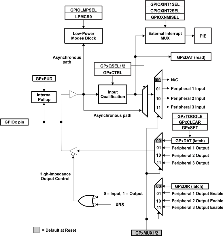
On the 280x, the GPIO MUX can multiplex up to three independent peripheral signals on a single GPIO pin in addition to providing individual pin bit-banging IO capability. The GPIO MUX block diagram per pin is shown in Figure 6-16. Because of the open-drain capabilities of the I2C pins, the GPIO MUX block diagram for these pins differ. See the TMS320x280x, 2801x, 2804x DSP system control and interrupts reference guide for details.

The 280x supports 34 GPIO pins. The GPIO control and data registers are mapped to Peripheral Frame 1 to enable 32-bit operations on the registers (along with 16-bit operations). Table 6-16 shows the GPIO register mapping.
Table 6-16 GPIO Registers
| NAME | ADDRESS | SIZE (x16) | DESCRIPTION |
|---|---|---|---|
| GPIO CONTROL REGISTERS (EALLOW PROTECTED) | |||
| GPACTRL | 0x6F80 | 2 | GPIO A Control Register (GPIO0 to 31) |
| GPAQSEL1 | 0x6F82 | 2 | GPIO A Qualifier Select 1 Register (GPIO0 to 15) |
| GPAQSEL2 | 0x6F84 | 2 | GPIO A Qualifier Select 2 Register (GPIO16 to 31) |
| GPAMUX1 | 0x6F86 | 2 | GPIO A MUX 1 Register (GPIO0 to 15) |
| GPAMUX2 | 0x6F88 | 2 | GPIO A MUX 2 Register (GPIO16 to 31) |
| GPADIR | 0x6F8A | 2 | GPIO A Direction Register (GPIO0 to 31) |
| GPAPUD | 0x6F8C | 2 | GPIO A Pull Up Disable Register (GPIO0 to 31) |
| Reserved | 0x6F8E –
0x6F8F |
2 | Reserved |
| GPBCTRL | 0x6F90 | 2 | GPIO B Control Register (GPIO32 to 35) |
| GPBQSEL1 | 0x6F92 | 2 | GPIO B Qualifier Select 1 Register (GPIO32 to 35) |
| GPBQSEL2 | 0x6F94 | 2 | Reserved |
| GPBMUX1 | 0x6F96 | 2 | GPIO B MUX 1 Register (GPIO32 to 35) |
| GPBMUX2 | 0x6F98 | 2 | Reserved |
| GPBDIR | 0x6F9A | 2 | GPIO B Direction Register (GPIO32 to 35) |
| GPBPUD | 0x6F9C | 2 | GPIO B Pull Up Disable Register (GPIO32 to 35) |
| Reserved | 0x6F9E –
0x6F9F |
2 | Reserved |
| Reserved | 0x6FA0 –
0x6FBF |
32 | Reserved |
| GPIO DATA REGISTERS (NOT EALLOW PROTECTED) | |||
| GPADAT | 0x6FC0 | 2 | GPIO Data Register (GPIO0 to 31) |
| GPASET | 0x6FC2 | 2 | GPIO Data Set Register (GPIO0 to 31) |
| GPACLEAR | 0x6FC4 | 2 | GPIO Data Clear Register (GPIO0 to 31) |
| GPATOGGLE | 0x6FC6 | 2 | GPIO Data Toggle Register (GPIO0 to 31) |
| GPBDAT | 0x6FC8 | 2 | GPIO Data Register (GPIO32 to 35) |
| GPBSET | 0x6FCA | 2 | GPIO Data Set Register (GPIO32 to 35) |
| GPBCLEAR | 0x6FCC | 2 | GPIO Data Clear Register (GPIO32 to 35) |
| GPBTOGGLE | 0x6FCE | 2 | GPIO Data Toggle Register (GPIO32 to 35) |
| Reserved | 0x6FD0 –
0x6FDF |
16 | Reserved |
| GPIO INTERRUPT AND LOW POWER MODES SELECT REGISTERS (EALLOW PROTECTED) | |||
| GPIOXINT1SEL | 0x6FE0 | 1 | XINT1 GPIO Input Select Register (GPIO0 to 31) |
| GPIOXINT2SEL | 0x6FE1 | 1 | XINT2 GPIO Input Select Register (GPIO0 to 31) |
| GPIOXNMISEL | 0x6FE2 | 1 | XNMI GPIO Input Select Register (GPIO0 to 31) |
| Reserved | 0x6FE3 –
0x6FE7 |
5 | Reserved |
| GPIOLPMSEL | 0x6FE8 | 2 | LPM GPIO Select Register (GPIO0 to 31) |
| Reserved | 0x6FEA –
0x6FFF |
22 | Reserved |
Table 6-17 F2808 GPIO MUX Table
| GPAMUX1/2(3)
REGISTER BITS |
DEFAULT AT RESET
PRIMARY I/O FUNCTION (GPxMUX1/2 BITS = 0,0) |
PERIPHERAL
SELECTION 1(1) (GPxMUX1/2 BITS = 0,1) |
PERIPHERAL
SELECTION 2 (GPxMUX1/2 BITS = 1,0) |
PERIPHERAL
SELECTION 3 (GPxMUX1/2 BITS = 1,1) |
|---|---|---|---|---|
| GPAMUX1 | ||||
| 1–0 | GPIO0 | EPWM1A (O) | Reserved(2) | Reserved(2) |
| 3–2 | GPIO1 | EPWM1B (O) | SPISIMOD (I/O) | Reserved(2) |
| 5–4 | GPIO2 | EPWM2A (O) | Reserved(2) | Reserved(2) |
| 7–6 | GPIO3 | EPWM2B (O) | SPISOMID (I/O) | Reserved(2) |
| 9–8 | GPIO4 | EPWM3A (O) | Reserved(2) | Reserved(2) |
| 11–10 | GPIO5 | EPWM3B (O) | SPICLKD (I/O) | ECAP1 (I/O) |
| 13–12 | GPIO6 | EPWM4A (O) | EPWMSYNCI (I) | EPWMSYNCO (O) |
| 15–14 | GPIO7 | EPWM4B (O) | SPISTED (I/O) | ECAP2 (I/O) |
| 17–16 | GPIO8 | EPWM5A (O) | CANTXB (O) | ADCSOCAO (O) |
| 19–18 | GPIO9 | EPWM5B (O) | SCITXDB (O) | ECAP3 (I/O) |
| 21–20 | GPIO10 | EPWM6A (O) | CANRXB (I) | ADCSOCBO (O) |
| 23–22 | GPIO11 | EPWM6B (O) | SCIRXDB (I) | ECAP4 (I/O) |
| 25–24 | GPIO12 | TZ1 (I) | CANTXB (O) | SPISIMOB (I/O) |
| 27–26 | GPIO13 | TZ2 (I) | CANRXB (I) | SPISOMIB (I/O) |
| 29–28 | GPIO14 | TZ3 (I) | SCITXDB (O) | SPICLKB (I/O) |
| 31–30 | GPIO15 | TZ4 (I) | SCIRXDB (I) | SPISTEB (I/O) |
| GPAMUX2 | ||||
| 1–0 | GPIO16 | SPISIMOA (I/O) | CANTXB (O) | TZ5 (I) |
| 3–2 | GPIO17 | SPISOMIA (I/O) | CANRXB (I) | TZ6 (I) |
| 5–4 | GPIO18 | SPICLKA (I/O) | SCITXDB (O) | Reserved(2) |
| 7–6 | GPIO19 | SPISTEA (I/O) | SCIRXDB (I) | Reserved(2) |
| 9–8 | GPIO20 | EQEP1A (I) | SPISIMOC (I/O) | CANTXB (O) |
| 11–10 | GPIO21 | EQEP1B (I) | SPISOMIC (I/O) | CANRXB (I) |
| 13–12 | GPIO22 | EQEP1S (I/O) | SPICLKC (I/O) | SCITXDB (O) |
| 15–14 | GPIO23 | EQEP1I (I/O) | SPISTEC (I/O) | SCIRXDB (I) |
| 17–16 | GPIO24 | ECAP1 (I/O) | EQEP2A (I) | SPISIMOB (I/O) |
| 19–18 | GPIO25 | ECAP2 (I/O) | EQEP2B (I) | SPISOMIB (I/O) |
| 21–20 | GPIO26 | ECAP3 (I/O) | EQEP2I (I/O) | SPICLKB (I/O) |
| 23–22 | GPIO27 | ECAP4 (I/O) | EQEP2S (I/O) | SPISTEB (I/O) |
| 25–24 | GPIO28 | SCIRXDA (I) | Reserved(2) | TZ5 (I) |
| 27–26 | GPIO29 | SCITXDA (O) | Reserved(2) | TZ6 (I) |
| 29–28 | GPIO30 | CANRXA (I) | Reserved(2) | Reserved(2) |
| 31–30 | GPIO31 | CANTXA (O) | Reserved(2) | Reserved(2) |
| GPBMUX1 | ||||
| 1–0 | GPIO32 | SDAA (I/OC) | EPWMSYNCI (I) | ADCSOCAO (O) |
| 3–2 | GPIO33 | SCLA (I/OC) | EPWMSYNCO (O) | ADCSOCBO (O) |
| 5–4 | GPIO34 | Reserved(2) | Reserved(2) | Reserved(2) |
The user can select the type of input qualification for each GPIO pin via the GPxQSEL1/2 registers from four choices:
- Synchronization To SYSCLKOUT Only (GPxQSEL1/2 = 0,0): This is the default mode of all GPIO pins at reset and it simply synchronizes the input signal to the system clock (SYSCLKOUT).
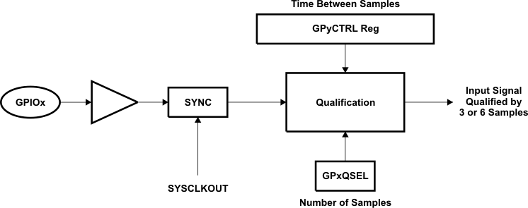
- Qualification Using Sampling Window (GPxQSEL1/2 = 0,1 and 1,0): In this mode the input signal, after synchronization to the system clock (SYSCLKOUT), is qualified by a specified number of cycles before the input is allowed to change.
- The sampling period is specified by the QUALPRD bits in the GPxCTRL register and is configurable in groups of 8 signals. It specifies a multiple of SYSCLKOUT cycles for sampling the input signal. The sampling window is either 3-samples or 6-samples wide and the output is only changed when ALL samples are the same (all 0s or all 1s) as shown in Figure 5-11 (for 6-sample mode).
- No Synchronization (GPxQSEL1/2 = 1,1): This mode is used for peripherals where synchronization is not required (synchronization is performed within the peripheral).
 Figure 6-17 Qualification Using Sampling Window
 Due to the multi-level multiplexing that is required on the 280x device, there may be cases where a peripheral input signal can be mapped to more then one GPIO pin. Also, when an input signal is not selected, the input signal will default to either a 0 or 1 state, depending on the peripheral.