ZHCS898O October 2003 – March 2019 TMS320F2801 , TMS320F28015 , TMS320F28016 , TMS320F2802 , TMS320F2806 , TMS320F2808 , TMS320F2809
PRODUCTION DATA.
- 1器件概述
- 2修订历史记录
- 3Device Comparison
- 4Terminal Configuration and Functions
-
5Specifications
- 5.1 Absolute Maximum Ratings
- 5.2 ESD Ratings – Automotive
- 5.3 ESD Ratings – Commercial
- 5.4 Recommended Operating Conditions
- 5.5
Power Consumption Summary
- Table 5-1 TMS320F2809, TMS320F2808 Current Consumption by Power-Supply Pins at 100-MHz SYSCLKOUT
- Table 5-2 TMS320F2806 Current Consumption by Power-Supply Pins at 100-MHz SYSCLKOUT
- Table 5-3 TMS320F2802, TMS320F2801 Current Consumption by Power-Supply Pins at 100-MHz SYSCLKOUT
- Table 5-4 TMS320C2802, TMS320C2801 Current Consumption by Power-Supply Pins at 100-MHz SYSCLKOUT
- 5.5.1 Reducing Current Consumption
- 5.5.2 Current Consumption Graphs
- 5.6 Electrical Characteristics
- 5.7 Thermal Resistance Characteristics for F280x 100-Ball GGM Package
- 5.8 Thermal Resistance Characteristics for F280x 100-Pin PZ Package
- 5.9 Thermal Resistance Characteristics for C280x 100-Ball GGM Package
- 5.10 Thermal Resistance Characteristics for C280x 100-Pin PZ Package
- 5.11 Thermal Resistance Characteristics for F2809 100-Ball GGM Package
- 5.12 Thermal Resistance Characteristics for F2809 100-Pin PZ Package
- 5.13 Thermal Design Considerations
- 5.14
Timing and Switching Characteristics
- 5.14.1 Timing Parameter Symbology
- 5.14.2 Power Sequencing
- 5.14.3 Clock Requirements and Characteristics
- 5.14.4
Peripherals
- 5.14.4.1 General-Purpose Input/Output (GPIO)
- 5.14.4.2 Enhanced Control Peripherals
- 5.14.4.3 External Interrupt Timing
- 5.14.4.4 I2C Electrical Specification and Timing
- 5.14.4.5 Serial Peripheral Interface (SPI) Timing
- 5.14.5 Emulator Connection Without Signal Buffering for the DSP
- 5.14.6 Flash Timing
- 5.15 On-Chip Analog-to-Digital Converter
- 5.16 Migrating From F280x Devices to C280x Devices
- 5.17 ROM Timing (C280x only)
-
6Detailed Description
- 6.1
Brief Descriptions
- 6.1.1 C28x CPU
- 6.1.2 Memory Bus (Harvard Bus Architecture)
- 6.1.3 Peripheral Bus
- 6.1.4 Real-Time JTAG and Analysis
- 6.1.5 Flash
- 6.1.6 ROM
- 6.1.7 M0, M1 SARAMs
- 6.1.8 L0, L1, H0 SARAMs
- 6.1.9 Boot ROM
- 6.1.10 Security
- 6.1.11 Peripheral Interrupt Expansion (PIE) Block
- 6.1.12 External Interrupts (XINT1, XINT2, XNMI)
- 6.1.13 Oscillator and PLL
- 6.1.14 Watchdog
- 6.1.15 Peripheral Clocking
- 6.1.16 Low-Power Modes
- 6.1.17 Peripheral Frames 0, 1, 2 (PFn)
- 6.1.18 General-Purpose Input/Output (GPIO) Multiplexer
- 6.1.19 32-Bit CPU-Timers (0, 1, 2)
- 6.1.20 Control Peripherals
- 6.1.21 Serial Port Peripherals
- 6.2
Peripherals
- 6.2.1 32-Bit CPU-Timers 0/1/2
- 6.2.2 Enhanced PWM Modules (ePWM1/2/3/4/5/6)
- 6.2.3 Hi-Resolution PWM (HRPWM)
- 6.2.4 Enhanced CAP Modules (eCAP1/2/3/4)
- 6.2.5 Enhanced QEP Modules (eQEP1/2)
- 6.2.6 Enhanced Analog-to-Digital Converter (ADC) Module
- 6.2.7 Enhanced Controller Area Network (eCAN) Modules (eCAN-A and eCAN-B)
- 6.2.8 Serial Communications Interface (SCI) Modules (SCI-A, SCI-B)
- 6.2.9 Serial Peripheral Interface (SPI) Modules (SPI-A, SPI-B, SPI-C, SPI-D)
- 6.2.10 Inter-Integrated Circuit (I2C)
- 6.2.11 GPIO MUX
- 6.3 Memory Maps
- 6.4 Register Map
- 6.5 Interrupts
- 6.6 System Control
- 6.7 Low-Power Modes Block
- 6.1
Brief Descriptions
- 7Applications, Implementation, and Layout
- 8器件和文档支持
- 9机械、封装和可订购信息
封装选项
请参考 PDF 数据表获取器件具体的封装图。
机械数据 (封装 | 引脚)
- PZ|100
散热焊盘机械数据 (封装 | 引脚)
- PZ|100
订购信息
6.5 Interrupts
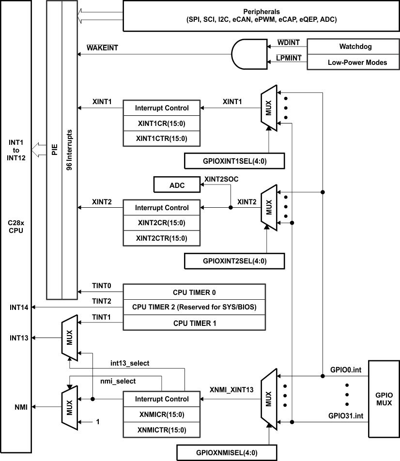
Figure 6-23 shows how the various interrupt sources are multiplexed within the 280x devices.
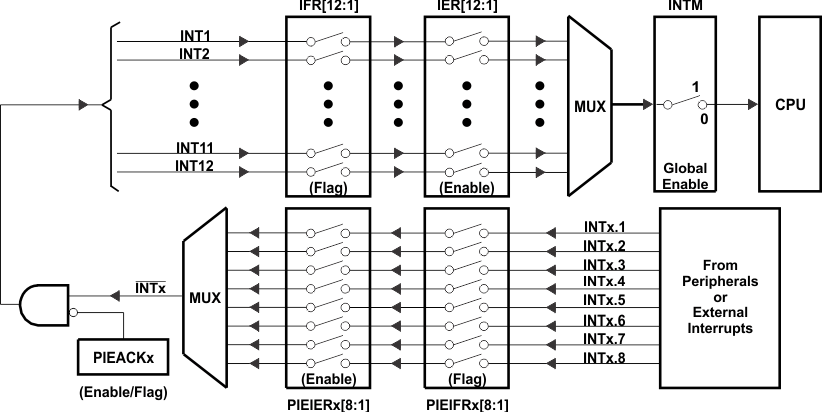
Eight PIE block interrupts are grouped into one CPU interrupt. In total, 12 CPU interrupt groups, with 8 interrupts per group equals 96 possible interrupts. On the 280x, 43 of these are used by peripherals as shown in Table 6-28.
The TRAP #VectorNumber instruction transfers program control to the interrupt service routine corresponding to the vector specified. TRAP #0 attempts to transfer program control to the address pointed to by the reset vector. The PIE vector table does not, however, include a reset vector. Therefore, TRAP #0 should not be used when the PIE is enabled. Doing so will result in undefined behavior.
When the PIE is enabled, TRAP #1 through TRAP #12 will transfer program control to the interrupt service routine corresponding to the first vector within the PIE group. For example: TRAP #1 fetches the vector from INT1.1, TRAP #2 fetches the vector from INT2.1 and so forth.
 Figure 6-23 External and PIE Interrupt Sources
  Figure 6-24 Multiplexing of Interrupts Using the PIE Block
 Table 6-28 PIE Peripheral Interrupts(1)
| CPU INTERRUPTS | PIE INTERRUPTS | |||||||
|---|---|---|---|---|---|---|---|---|
| INTx.8 | INTx.7 | INTx.6 | INTx.5 | INTx.4 | INTx.3 | INTx.2 | INTx.1 | |
| INT1 | WAKEINT
(LPM/WD) |
TINT0
(TIMER 0) |
ADCINT(2)
(ADC) |
XINT2 | XINT1 | Reserved | SEQ2INT
(ADC) |
SEQ1INT
(ADC) |
| INT2 | Reserved | Reserved | EPWM6_TZINT
(ePWM6) |
EPWM5_TZINT
(ePWM5) |
EPWM4_TZINT
(ePWM4) |
EPWM3_TZINT
(ePWM3) |
EPWM2_TZINT
(ePWM2) |
EPWM1_TZINT
(ePWM1) |
| INT3 | Reserved | Reserved | EPWM6_INT
(ePWM6) |
EPWM5_INT
(ePWM5) |
EPWM4_INT
(ePWM4) |
EPWM3_INT
(ePWM3) |
EPWM2_INT
(ePWM2) |
EPWM1_INT
(ePWM1) |
| INT4 | Reserved | Reserved | Reserved | Reserved | ECAP4_INT
(eCAP4) |
ECAP3_INT
(eCAP3) |
ECAP2_INT
(eCAP2) |
ECAP1_INT
(eCAP1) |
| INT5 | Reserved | Reserved | Reserved | Reserved | Reserved | Reserved | EQEP2_INT
(eQEP2) |
EQEP1_INT
(eQEP1) |
| INT6 | SPITXINTD
(SPI-D) |
SPIRXINTD
(SPI-D) |
SPITXINTC
(SPI-C) |
SPIRXINTC
(SPI-C) |
SPITXINTB
(SPI-B) |
SPIRXINTB
(SPI-B) |
SPITXINTA
(SPI-A) |
SPIRXINTA
(SPI-A) |
| INT7 | Reserved | Reserved | Reserved | Reserved | Reserved | Reserved | Reserved | Reserved |
| INT8 | Reserved | Reserved | Reserved | Reserved | Reserved | Reserved | I2CINT2A
(I2C-A) |
I2CINT1A
(I2C-A) |
| INT9 | ECAN1_INTB
(CAN-B) |
ECAN0_INTB
(CAN-B) |
ECAN1_INTA
(CAN-A) |
ECAN0_INTA
(CAN-A) |
SCITXINTB
(SCI-B) |
SCIRXINTB
(SCI-B) |
SCITXINTA
(SCI-A) |
SCIRXINTA
(SCI-A) |
| INT10 | Reserved | Reserved | Reserved | Reserved | Reserved | Reserved | Reserved | Reserved |
| INT11 | Reserved | Reserved | Reserved | Reserved | Reserved | Reserved | Reserved | Reserved |
| INT12 | Reserved | Reserved | Reserved | Reserved | Reserved | Reserved | Reserved | Reserved |
1) No peripheral within the group is asserting interrupts.
2) No peripheral interrupts are assigned to the group (example PIE group 12).
Table 6-29 PIE Configuration and Control Registers
| NAME | ADDRESS | SIZE (x16) | DESCRIPTION(1) |
|---|---|---|---|
| PIECTRL | 0x0CE0 | 1 | PIE, Control Register |
| PIEACK | 0x0CE1 | 1 | PIE, Acknowledge Register |
| PIEIER1 | 0x0CE2 | 1 | PIE, INT1 Group Enable Register |
| PIEIFR1 | 0x0CE3 | 1 | PIE, INT1 Group Flag Register |
| PIEIER2 | 0x0CE4 | 1 | PIE, INT2 Group Enable Register |
| PIEIFR2 | 0x0CE5 | 1 | PIE, INT2 Group Flag Register |
| PIEIER3 | 0x0CE6 | 1 | PIE, INT3 Group Enable Register |
| PIEIFR3 | 0x0CE7 | 1 | PIE, INT3 Group Flag Register |
| PIEIER4 | 0x0CE8 | 1 | PIE, INT4 Group Enable Register |
| PIEIFR4 | 0x0CE9 | 1 | PIE, INT4 Group Flag Register |
| PIEIER5 | 0x0CEA | 1 | PIE, INT5 Group Enable Register |
| PIEIFR5 | 0x0CEB | 1 | PIE, INT5 Group Flag Register |
| PIEIER6 | 0x0CEC | 1 | PIE, INT6 Group Enable Register |
| PIEIFR6 | 0x0CED | 1 | PIE, INT6 Group Flag Register |
| PIEIER7 | 0x0CEE | 1 | PIE, INT7 Group Enable Register |
| PIEIFR7 | 0x0CEF | 1 | PIE, INT7 Group Flag Register |
| PIEIER8 | 0x0CF0 | 1 | PIE, INT8 Group Enable Register |
| PIEIFR8 | 0x0CF1 | 1 | PIE, INT8 Group Flag Register |
| PIEIER9 | 0x0CF2 | 1 | PIE, INT9 Group Enable Register |
| PIEIFR9 | 0x0CF3 | 1 | PIE, INT9 Group Flag Register |
| PIEIER10 | 0x0CF4 | 1 | PIE, INT10 Group Enable Register |
| PIEIFR10 | 0x0CF5 | 1 | PIE, INT10 Group Flag Register |
| PIEIER11 | 0x0CF6 | 1 | PIE, INT11 Group Enable Register |
| PIEIFR11 | 0x0CF7 | 1 | PIE, INT11 Group Flag Register |
| PIEIER12 | 0x0CF8 | 1 | PIE, INT12 Group Enable Register |
| PIEIFR12 | 0x0CF9 | 1 | PIE, INT12 Group Flag Register |
| Reserved | 0x0CFA –
0x0CFF |
6 | Reserved |