ZHCSA13P November 2008 – February 2021 TMS320F28020 , TMS320F280200 , TMS320F28021 , TMS320F28022 , TMS320F28023 , TMS320F28023-Q1 , TMS320F28026 , TMS320F28026-Q1 , TMS320F28026F , TMS320F28027 , TMS320F28027-Q1 , TMS320F28027F , TMS320F28027F-Q1
PRODUCTION DATA
- 1 特性
- 2 应用
- 3 说明
- 4 功能方框图
- 5 修订历史记录
- 6 Device Comparison
- 7 Terminal Configuration and Functions
- 8 规格
-
9 详细说明
- 9.1
Overview
- 9.1.1 CPU
- 9.1.2 Memory Bus (Harvard Bus Architecture)
- 9.1.3 外设总线
- 9.1.4 Real-Time JTAG and Analysis
- 9.1.5 Flash
- 9.1.6 M0,M1 SARAM
- 9.1.7 L0 SARAM
- 9.1.8 Boot ROM
- 9.1.9 Security
- 9.1.10 外设中断扩展 (PIE) 块
- 9.1.11 外部中断 (XINT1-XINT3)
- 9.1.12 内部零引脚振荡器、振荡器和 PLL
- 9.1.13 看门狗
- 9.1.14 Peripheral Clocking
- 9.1.15 Low-power Modes
- 9.1.16 外设帧 0,1,2 (PFn)
- 9.1.17 通用输入/输出 (GPIO) 复用器
- 9.1.18 32 位 CPU 定时器 (0,1,2)
- 9.1.19 Control Peripherals
- 9.1.20 串行端口外设
- 9.2 Memory Maps
- 9.3 Register Maps
- 9.4 Device Emulation Registers
- 9.5 VREG/BOR/POR
- 9.6 系统控制
- 9.7 Low-power Modes Block
- 9.8 Interrupts
- 9.9
外设
- 9.9.1 Analog Block
- 9.9.2 详细说明
- 9.9.3 Serial Peripheral Interface (SPI) Module
- 9.9.4 Serial Communications Interface (SCI) Module
- 9.9.5 Inter-Integrated Circuit (I2C)
- 9.9.6 Enhanced PWM Modules (ePWM1/2/3/4)
- 9.9.7 High-Resolution PWM (HRPWM)
- 9.9.8 Enhanced Capture Module (eCAP1)
- 9.9.9 JTAG 端口
- 9.9.10 General-Purpose Input/Output (GPIO) MUX
- 9.1
Overview
- 10应用、实施和布局
- 11器件和文档支持
- 12机械、封装和可订购信息
封装选项
机械数据 (封装 | 引脚)
散热焊盘机械数据 (封装 | 引脚)
- DA|38
订购信息
9.6.2 Crystal Oscillator Option
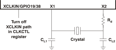
The on-chip crystal oscillator X1 and X2 pins are 1.8-V level signals and must never have 3.3-V level signals applied to them. If a system 3.3-V external oscillator is to be used as a clock source, it should be connected to the XCLKIN pin only. The X1 pin is not intended to be used as a single-ended clock input, it should be used with X2 and a crystal.
The typical specifications for the external quartz crystal (fundamental mode, parallel resonant) are listed in Table 9-13. Furthermore, ESR range = 30 to 150 Ω.
| FREQUENCY (MHz) | Rd (Ω) | CL1 (pF) | CL2 (pF) |
|---|---|---|---|
| 5 | 2200 | 18 | 18 |
| 10 | 470 | 15 | 15 |
| 15 | 0 | 15 | 15 |
| 20 | 0 | 12 | 12 |

- CL1 and CL2 are the total capacitance of the circuit board and components excluding the IC and crystal. The value is usually approximately twice the value of the crystal's load capacitance.
- The load capacitance of the crystal is described in the crystal specifications of the manufacturers.
- TI recommends that customers have the resonator/crystal vendor characterize the operation of their device with the MCU chip. The resonator/crystal vendor has the equipment and expertise to tune the tank circuit. The vendor can also advise the customer regarding the proper tank component values that will produce proper start-up and stability over the entire operating range.
 Figure 9-10 Using a
3.3-V External Oscillator