ZHCSA13P November 2008 – February 2021 TMS320F28020 , TMS320F280200 , TMS320F28021 , TMS320F28022 , TMS320F28023 , TMS320F28023-Q1 , TMS320F28026 , TMS320F28026-Q1 , TMS320F28026F , TMS320F28027 , TMS320F28027-Q1 , TMS320F28027F , TMS320F28027F-Q1
PRODUCTION DATA
- 1 特性
- 2 应用
- 3 说明
- 4 功能方框图
- 5 修订历史记录
- 6 Device Comparison
- 7 Terminal Configuration and Functions
- 8 规格
-
9 详细说明
- 9.1
Overview
- 9.1.1 CPU
- 9.1.2 Memory Bus (Harvard Bus Architecture)
- 9.1.3 外设总线
- 9.1.4 Real-Time JTAG and Analysis
- 9.1.5 Flash
- 9.1.6 M0,M1 SARAM
- 9.1.7 L0 SARAM
- 9.1.8 Boot ROM
- 9.1.9 Security
- 9.1.10 外设中断扩展 (PIE) 块
- 9.1.11 外部中断 (XINT1-XINT3)
- 9.1.12 内部零引脚振荡器、振荡器和 PLL
- 9.1.13 看门狗
- 9.1.14 Peripheral Clocking
- 9.1.15 Low-power Modes
- 9.1.16 外设帧 0,1,2 (PFn)
- 9.1.17 通用输入/输出 (GPIO) 复用器
- 9.1.18 32 位 CPU 定时器 (0,1,2)
- 9.1.19 Control Peripherals
- 9.1.20 串行端口外设
- 9.2 Memory Maps
- 9.3 Register Maps
- 9.4 Device Emulation Registers
- 9.5 VREG/BOR/POR
- 9.6 系统控制
- 9.7 Low-power Modes Block
- 9.8 Interrupts
- 9.9
外设
- 9.9.1 Analog Block
- 9.9.2 详细说明
- 9.9.3 Serial Peripheral Interface (SPI) Module
- 9.9.4 Serial Communications Interface (SCI) Module
- 9.9.5 Inter-Integrated Circuit (I2C)
- 9.9.6 Enhanced PWM Modules (ePWM1/2/3/4)
- 9.9.7 High-Resolution PWM (HRPWM)
- 9.9.8 Enhanced Capture Module (eCAP1)
- 9.9.9 JTAG 端口
- 9.9.10 General-Purpose Input/Output (GPIO) MUX
- 9.1
Overview
- 10应用、实施和布局
- 11器件和文档支持
- 12机械、封装和可订购信息
9.5.2 On-chip Power-On Reset (POR) and Brown-Out Reset (BOR) Circuit
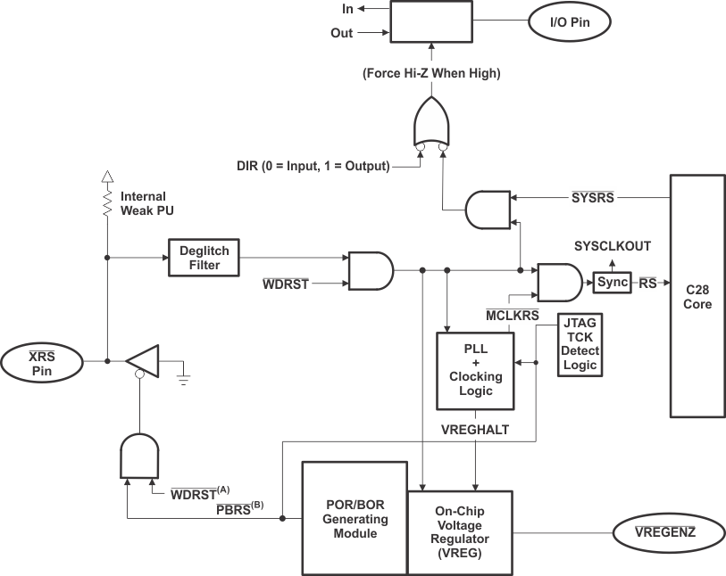
Two on-chip supervisory circuits, the power-on reset (POR) and the brown-out reset (BOR) remove the burden of monitoring the VDD and VDDIO supply rails from the application board. The purpose of the POR is to create a clean reset throughout the device during the entire power-up procedure. The trip point is a looser, lower trip point than the BOR, which watches for dips in the VDD or VDDIO rail during device operation. The POR function is present on both VDD and VDDIO rails at all times. After initial device power-up, the BOR function is present on VDDIO at all times, and on VDD when the internal VREG is enabled ( VREGENZ pin is tied low). Both functions tie the XRS pin low when one of the voltages is below their respective trip point. VDD BOR and overvoltage trip points are outside of the recommended operating voltages. Proper device operation cannot be ensured. If overvoltage or undervoltage conditions affecting the system is a concern for an application, an external voltage supervisor should be added. Figure 9-6 shows the VREG, POR, and BOR. To disable both the VDD and VDDIO BOR functions, a bit is provided in the BORCFG register. For details, see the System Control chapter in the TMS320F2802x,TMS320F2802xx Technical Reference Manual.
