ZHCSIE4A June   2018  – July 2018 TMS320F28035-EP

PRODUCTION DATA.  

  1. 1器件概述
    1. 1.1 特性
    2. 1.2 应用范围
    3. 1.3 说明
    4. 1.4 功能方框图
  2. 2修订历史记录
  3. 3Terminal Configuration and Functions
    1. 3.1 Pin Diagram
    2. 3.2 Signal Descriptions
      1. Table 3-1 Signal Descriptions
  4. 4Specifications
    1. 4.1  Absolute Maximum Ratings
    2. 4.2  ESD Ratings
    3. 4.3  Power-On Hours (POH) Limits
    4. 4.4  Recommended Operating Conditions
    5. 4.5  Power Consumption Summary
      1. Table 4-1 TMS320F2803x Current Consumption at 60-MHz SYSCLKOUT
      2. 4.5.1     Reducing Current Consumption
      3. 4.5.2     Current Consumption Graphs (VREG Enabled)
    6. 4.6  Electrical Characteristics
    7. 4.7  Thermal Resistance Characteristics
    8. 4.8  Thermal Design Considerations
    9. 4.9  Emulator Connection Without Signal Buffering for the MCU
    10. 4.10 Parameter Information
      1. 4.10.1 Timing Parameter Symbology
      2. 4.10.2 General Notes on Timing Parameters
    11. 4.11 Test Load Circuit
    12. 4.12 Power Sequencing
      1. Table 4-4 Reset (XRS) Timing Requirements
      2. Table 4-5 Reset (XRS) Switching Characteristics
    13. 4.13 Clock Specifications
      1. 4.13.1 Device Clock Table
        1. Table 4-6 2803x Clock Table and Nomenclature (60-MHz Devices)
        2. Table 4-7 Device Clocking Requirements/Characteristics
        3. Table 4-8 Internal Zero-Pin Oscillator (INTOSC1/INTOSC2) Characteristics
      2. 4.13.2 Clock Requirements and Characteristics
        1. Table 4-9  XCLKIN Timing Requirements – PLL Enabled
        2. Table 4-10 XCLKIN Timing Requirements – PLL Disabled
        3. Table 4-11 XCLKOUT Switching Characteristics (PLL Bypassed or Enabled)
    14. 4.14 Flash Timing
      1. Table 4-12 Flash/OTP Endurance
      2. Table 4-13 Flash Parameters at 60-MHz SYSCLKOUT
      3. Table 4-14 Flash/OTP Access Timing
      4. Table 4-15 Flash Data Retention Duration
  5. 5Detailed Description
    1. 5.1 Overview
      1. 5.1.1  CPU
      2. 5.1.2  Control Law Accelerator (CLA)
      3. 5.1.3  Memory Bus (Harvard Bus Architecture)
      4. 5.1.4  Peripheral Bus
      5. 5.1.5  Real-Time JTAG and Analysis
      6. 5.1.6  Flash
      7. 5.1.7  M0, M1 SARAMs
      8. 5.1.8  L0 SARAM, and L1, L2, and L3 DPSARAMs
      9. 5.1.9  Boot ROM
        1. 5.1.9.1 Emulation Boot
        2. 5.1.9.2 GetMode
        3. 5.1.9.3 Peripheral Pins Used by the Bootloader
      10. 5.1.10 Security
      11. 5.1.11 Peripheral Interrupt Expansion (PIE) Block
      12. 5.1.12 External Interrupts (XINT1–XINT3)
      13. 5.1.13 Internal Zero Pin Oscillators, Oscillator, and PLL
      14. 5.1.14 Watchdog
      15. 5.1.15 Peripheral Clocking
      16. 5.1.16 Low-power Modes
      17. 5.1.17 Peripheral Frames 0, 1, 2, 3 (PFn)
      18. 5.1.18 General-Purpose Input/Output (GPIO) Multiplexer
      19. 5.1.19 32-Bit CPU-Timers (0, 1, 2)
      20. 5.1.20 Control Peripherals
      21. 5.1.21 Serial Port Peripherals
    2. 5.2 Memory Maps
    3. 5.3 Register Maps
    4. 5.4 Device Emulation Registers
    5. 5.5 VREG/BOR/POR
      1. 5.5.1 On-chip Voltage Regulator (VREG)
        1. 5.5.1.1 Using the On-chip VREG
        2. 5.5.1.2 Disabling the On-chip VREG
      2. 5.5.2 On-chip Power-On Reset (POR) and Brown-Out Reset (BOR) Circuit
    6. 5.6 System Control
      1. 5.6.1 Internal Zero Pin Oscillators
      2. 5.6.2 Crystal Oscillator Option
      3. 5.6.3 PLL-Based Clock Module
      4. 5.6.4 Loss of Input Clock (NMI Watchdog Function)
      5. 5.6.5 CPU-Watchdog Module
    7. 5.7 Low-Power Modes Block
    8. 5.8 Interrupts
      1. 5.8.1 External Interrupts
        1. 5.8.1.1 External Interrupt Electrical Data/Timing
          1. Table 5-20 External Interrupt Timing Requirements
          2. Table 5-21 External Interrupt Switching Characteristics
    9. 5.9 Peripherals
      1. 5.9.1  Control Law Accelerator (CLA) Overview
      2. 5.9.2  Analog Block
        1. 5.9.2.1 Analog-to-Digital Converter (ADC)
          1. 5.9.2.1.1 Features
          2. 5.9.2.1.2 ADC Start-of-Conversion Electrical Data/Timing
            1. Table 5-26 External ADC Start-of-Conversion Switching Characteristics
          3. 5.9.2.1.3 On-Chip Analog-to-Digital Converter (ADC) Electrical Data/Timing
            1. Table 5-27  ADC Electrical Characteristics
            2. Table 5-28  ADC Power Modes
            3. 5.9.2.1.3.1 Internal Temperature Sensor
              1. Table 5-29 Temperature Sensor Coefficient
            4. 5.9.2.1.3.2 ADC Power-Up Control Bit Timing
              1. Table 5-30 ADC Power-Up Delays
            5. 5.9.2.1.3.3 ADC Sequential and Simultaneous Timings
        2. 5.9.2.2 ADC MUX
        3. 5.9.2.3 Comparator Block
          1. 5.9.2.3.1 On-Chip Comparator/DAC Electrical Data/Timing
            1. Table 5-32 Electrical Characteristics of the Comparator/DAC
      3. 5.9.3  Detailed Descriptions
      4. 5.9.4  Serial Peripheral Interface (SPI) Module
        1. 5.9.4.1 SPI Master Mode Electrical Data/Timing
          1. Table 5-35 SPI Master Mode External Timing (Clock Phase = 0)
          2. Table 5-36 SPI Master Mode External Timing (Clock Phase = 1)
        2. 5.9.4.2 SPI Slave Mode Electrical Data/Timing
          1. Table 5-37 SPI Slave Mode External Timing (Clock Phase = 0)
          2. Table 5-38 SPI Slave Mode External Timing (Clock Phase = 1)
      5. 5.9.5  Serial Communications Interface (SCI) Module
      6. 5.9.6  Local Interconnect Network (LIN)
      7. 5.9.7  Enhanced Controller Area Network (eCAN) Module
      8. 5.9.8  Inter-Integrated Circuit (I2C)
        1. 5.9.8.1 I2C Electrical Data/Timing
          1. Table 5-44 I2C Timing Requirements
          2. Table 5-45 I2C Switching Characteristics
      9. 5.9.9  Enhanced PWM Modules (ePWM1/2/3/4/5/6/7)
        1. 5.9.9.1 ePWM Electrical Data/Timing
          1. Table 5-48 ePWM Timing Requirements
          2. Table 5-49 ePWM Switching Characteristics
        2. 5.9.9.2 Trip-Zone Input Timing
          1. Table 5-50 Trip-Zone Input Timing Requirements
      10. 5.9.10 High-Resolution PWM (HRPWM)
        1. 5.9.10.1 HRPWM Electrical Data/Timing
          1. Table 5-51 High-Resolution PWM Characteristics
      11. 5.9.11 Enhanced Capture Module (eCAP1)
        1. 5.9.11.1 eCAP Electrical Data/Timing
          1. Table 5-53 Enhanced Capture (eCAP) Timing Requirement
          2. Table 5-54 eCAP Switching Characteristics
      12. 5.9.12 High-Resolution Capture (HRCAP) Module
        1. 5.9.12.1 HRCAP Electrical Data/Timing
          1. Table 5-56 High-Resolution Capture (HRCAP) Timing Requirements
      13. 5.9.13 Enhanced Quadrature Encoder Pulse (eQEP)
        1. 5.9.13.1 eQEP Electrical Data/Timing
          1. Table 5-58 Enhanced Quadrature Encoder Pulse (eQEP) Timing Requirements
          2. Table 5-59 eQEP Switching Characteristics
      14. 5.9.14 JTAG Port
      15. 5.9.15 General-Purpose Input/Output (GPIO) MUX
        1. 5.9.15.1 GPIO Electrical Data/Timing
          1. 5.9.15.1.1 GPIO - Output Timing
            1. Table 5-63 General-Purpose Output Switching Characteristics
          2. 5.9.15.1.2 GPIO - Input Timing
            1. Table 5-64 General-Purpose Input Timing Requirements
          3. 5.9.15.1.3 Sampling Window Width for Input Signals
          4. 5.9.15.1.4 Low-Power Mode Wakeup Timing
            1. Table 5-65 IDLE Mode Timing Requirements
            2. Table 5-66 IDLE Mode Switching Characteristics
            3. Table 5-67 STANDBY Mode Timing Requirements
            4. Table 5-68 STANDBY Mode Switching Characteristics
            5. Table 5-69 HALT Mode Timing Requirements
            6. Table 5-70 HALT Mode Switching Characteristics
  6. 6Applications, Implementation, and Layout
    1. 6.1 TI Design or Reference Design
  7. 7器件和文档支持
    1. 7.1 使用入门
    2. 7.2 器件和开发支持工具命名规则
    3. 7.3 工具和软件
    4. 7.4 文档支持
    5. 7.5 Community Resources
    6. 7.6 商标
    7. 7.7 静电放电警告
    8. 7.8 术语表
  8. 8机械、封装和可订购信息
    1. 8.1 封装信息

封装选项

机械数据 (封装 | 引脚)
散热焊盘机械数据 (封装 | 引脚)
订购信息

Table 5-38 SPI Slave Mode External Timing (Clock Phase = 1)(1)(2)(3)(4)

NO. PARAMETER MIN MAX UNIT
12 tc(SPC)S Cycle time, SPICLK 4tc(SYSCLK) ns
13 tw(SPC1)S Pulse duration, SPICLK first pulse 2tc(SYSCLK) – 1 ns
14 tw(SPC2)S Pulse duration, SPICLK second pulse 2tc(SYSCLK) – 1 ns
17 td(SOMI)S Delay time, SPICLK to SPISOMI valid 21 ns
18 tv(SOMI)S Valid time, SPISOMI data valid after SPICLK 0 ns
21 tsu(SIMO)S Setup time, SPISIMO valid before SPICLK 1.5tc(SYSCLK) ns
22 th(SIMO)S Hold time, SPISIMO data valid after SPICLK 1.5tc(SYSCLK) ns
25 tsu(STE)S Setup time, SPISTE active before SPICLK 1.5tc(SYSCLK) ns
26 th(STE)S Hold time, SPISTE inactive after SPICLK 1.5tc(SYSCLK) ns
The MASTER / SLAVE bit (SPICTL.2) is cleared and the CLOCK PHASE bit (SPICTL.3) is cleared.
tc(SPC) = SPI clock cycle time = LSPCLK/4 or LSPCLK/(SPIBRR + 1).
Internal clock prescalers must be adjusted such that the SPI clock speed is limited to the following SPI clock rate:
Master mode transmit 25-MHz MAX, master mode receive 12.5-MHz MAX
Slave mode transmit 12.5-MHz MAX, slave mode receive 12.5-MHz MAX.
The active edge of the SPICLK signal referenced is controlled by the CLOCK POLARITY bit (SPICCR.6).
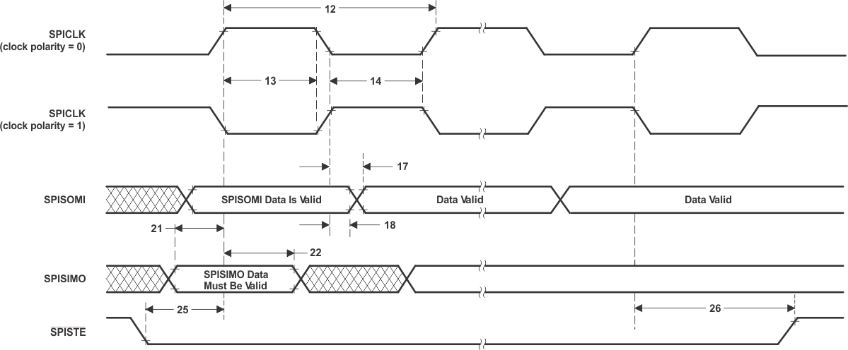
TMS320F28035-EP td_slave1_prs230.gifFigure 5-29 SPI Slave Mode External Timing (Clock Phase = 1)