ZHCSIE4A June 2018 – July 2018 TMS320F28035-EP
PRODUCTION DATA.
- 1器件概述
- 2修订历史记录
- 3Terminal Configuration and Functions
-
4Specifications
- 4.1 Absolute Maximum Ratings
- 4.2 ESD Ratings
- 4.3 Power-On Hours (POH) Limits
- 4.4 Recommended Operating Conditions
- 4.5 Power Consumption Summary
- 4.6 Electrical Characteristics
- 4.7 Thermal Resistance Characteristics
- 4.8 Thermal Design Considerations
- 4.9 Emulator Connection Without Signal Buffering for the MCU
- 4.10 Parameter Information
- 4.11 Test Load Circuit
- 4.12 Power Sequencing
- 4.13 Clock Specifications
- 4.14 Flash Timing
-
5Detailed Description
- 5.1
Overview
- 5.1.1 CPU
- 5.1.2 Control Law Accelerator (CLA)
- 5.1.3 Memory Bus (Harvard Bus Architecture)
- 5.1.4 Peripheral Bus
- 5.1.5 Real-Time JTAG and Analysis
- 5.1.6 Flash
- 5.1.7 M0, M1 SARAMs
- 5.1.8 L0 SARAM, and L1, L2, and L3 DPSARAMs
- 5.1.9 Boot ROM
- 5.1.10 Security
- 5.1.11 Peripheral Interrupt Expansion (PIE) Block
- 5.1.12 External Interrupts (XINT1–XINT3)
- 5.1.13 Internal Zero Pin Oscillators, Oscillator, and PLL
- 5.1.14 Watchdog
- 5.1.15 Peripheral Clocking
- 5.1.16 Low-power Modes
- 5.1.17 Peripheral Frames 0, 1, 2, 3 (PFn)
- 5.1.18 General-Purpose Input/Output (GPIO) Multiplexer
- 5.1.19 32-Bit CPU-Timers (0, 1, 2)
- 5.1.20 Control Peripherals
- 5.1.21 Serial Port Peripherals
- 5.2 Memory Maps
- 5.3 Register Maps
- 5.4 Device Emulation Registers
- 5.5 VREG/BOR/POR
- 5.6 System Control
- 5.7 Low-Power Modes Block
- 5.8 Interrupts
- 5.9
Peripherals
- 5.9.1 Control Law Accelerator (CLA) Overview
- 5.9.2 Analog Block
- 5.9.3 Detailed Descriptions
- 5.9.4 Serial Peripheral Interface (SPI) Module
- 5.9.5 Serial Communications Interface (SCI) Module
- 5.9.6 Local Interconnect Network (LIN)
- 5.9.7 Enhanced Controller Area Network (eCAN) Module
- 5.9.8 Inter-Integrated Circuit (I2C)
- 5.9.9 Enhanced PWM Modules (ePWM1/2/3/4/5/6/7)
- 5.9.10 High-Resolution PWM (HRPWM)
- 5.9.11 Enhanced Capture Module (eCAP1)
- 5.9.12 High-Resolution Capture (HRCAP) Module
- 5.9.13 Enhanced Quadrature Encoder Pulse (eQEP)
- 5.9.14 JTAG Port
- 5.9.15 General-Purpose Input/Output (GPIO) MUX
- 5.1
Overview
- 6Applications, Implementation, and Layout
- 7器件和文档支持
- 8机械、封装和可订购信息
5.9.6 Local Interconnect Network (LIN)
The device contains one LIN controller. The LIN standard is based on the SCI (UART) serial data link format. The LIN module can be configured to work as a SCI as well.
The LIN module has the following features:
- Compatible to LIN 1.3 or 2.0 protocols
- Two external pins: LINRX and LINTX
- Multibuffered receive and transmit units
- Identification masks for message filtering
- Automatic master header generation
- Programmable sync break field
- Sync field
- Identifier field
- Slave automatic synchronization
- Sync break detection
- Optional baudrate update
- Synchronization validation
- 231 programmable transmission rates with 7 fractional bits
- Wakeup on LINRX dominant level from transceiver
- Automatic wakeup support
- Wakeup signal generation
- Expiration times on wakeup signals
- Automatic bus idle detection
- Error detection
- Bit error
- Bus error
- No-response error
- Checksum error
- Sync field error
- Parity error
- 2 Interrupt lines with priority encoding for:
- Receive
- Transmit
- ID, error and status
NOTE
The 2803x devices have passed LIN 2.0 conformance tests (master and slave). Contact TI for details.
For more information on the LIN, see the TMS320F2803x Piccolo Local Interconnect Network (LIN) Module User's Guide.
The registers in Table 5-40 configure and control the operation of the LIN module.
Table 5-40 LIN-A Registers(1)
| NAME | ADDRESS | SIZE (x16) | DESCRIPTION |
|---|---|---|---|
| SCIGCR0 | 0x6C00 | 2 | Global Control Register 0 |
| SCIGCR1 | 0x6C02 | 2 | Global Control Register 1 |
| SCIGCR2 | 0x6C04 | 2 | Global Control Register 2 |
| SCISETINT | 0x6C06 | 2 | Interrupt Enable Register |
| SCICLEARINT | 0x6C08 | 2 | Interrupt Disable Register |
| SCISETINTLVL | 0x6C0A | 2 | Set Interrupt Level Register |
| SCICLEARINTLVL | 0x6C0C | 2 | Clear Interrupt Level Register |
| SCIFLR | 0x6C0E | 2 | Flag Register |
| SCIINTVECT0 | 0x6C10 | 2 | Interrupt Vector Offset Register 0 |
| SCIINTVECT1 | 0x6C12 | 2 | Interrupt Vector Offset Register 1 |
| SCIFORMAT | 0x6C14 | 2 | Length Control register |
| BRSR | 0x6C16 | 2 | Baud Rate Selection Register |
| SCIED | 0x6C18 | 2 | Emulation buffer register |
| SCIRD | 0x6C1A | 2 | Receiver data buffer register |
| SCITD | 0x6C1C | 2 | Transmit data buffer register |
| Reserved | 0x6C1E | 4 | RSVD |
| SIPIO2 | 0x6C22 | 2 | Pin control register 2 |
| Reserved | 0x6C24 | 10 | RSVD |
| LINCOMP | 0x6C30 | 2 | Compare register |
| LINRD0 | 0x6C32 | 2 | Receive data register 0 |
| LINRD1 | 0x6C34 | 2 | Receive data register 1 |
| LINMASK | 0x6C36 | 2 | Acceptance mask register |
| LINID | 0x6C38 | 2 | Register containing ID- byte, ID-SlaveTask byte, and ID received fields. |
| LINTD0 | 0x6C3A | 2 | Transmit Data Register 0 |
| LINTD1 | 0x6C3C | 2 | Transmit Data Register 1 |
| MBRSR | 0x6C3E | 2 | Baud Rate Selection Register |
| Reserved | 0x6C40 | 8 | RSVD |
| IODFTCTRL | 0x6C48 | 2 | IODFT for BLIN |
(1) Some registers and some bits in other registers are EALLOW-protected. See the TMS320F2803x Piccolo Local Interconnect Network (LIN) Module User's Guide for more details.
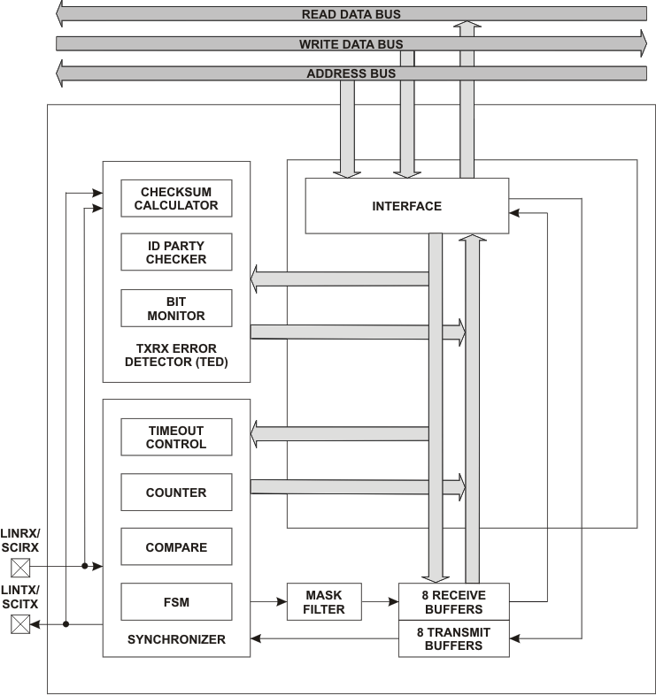
Figure 5-31 shows the LIN module block diagram.
 Figure 5-31 LIN Block Diagram