ZHCSIE4A June 2018 – July 2018 TMS320F28035-EP
PRODUCTION DATA.
- 1器件概述
- 2修订历史记录
- 3Terminal Configuration and Functions
-
4Specifications
- 4.1 Absolute Maximum Ratings
- 4.2 ESD Ratings
- 4.3 Power-On Hours (POH) Limits
- 4.4 Recommended Operating Conditions
- 4.5 Power Consumption Summary
- 4.6 Electrical Characteristics
- 4.7 Thermal Resistance Characteristics
- 4.8 Thermal Design Considerations
- 4.9 Emulator Connection Without Signal Buffering for the MCU
- 4.10 Parameter Information
- 4.11 Test Load Circuit
- 4.12 Power Sequencing
- 4.13 Clock Specifications
- 4.14 Flash Timing
-
5Detailed Description
- 5.1
Overview
- 5.1.1 CPU
- 5.1.2 Control Law Accelerator (CLA)
- 5.1.3 Memory Bus (Harvard Bus Architecture)
- 5.1.4 Peripheral Bus
- 5.1.5 Real-Time JTAG and Analysis
- 5.1.6 Flash
- 5.1.7 M0, M1 SARAMs
- 5.1.8 L0 SARAM, and L1, L2, and L3 DPSARAMs
- 5.1.9 Boot ROM
- 5.1.10 Security
- 5.1.11 Peripheral Interrupt Expansion (PIE) Block
- 5.1.12 External Interrupts (XINT1–XINT3)
- 5.1.13 Internal Zero Pin Oscillators, Oscillator, and PLL
- 5.1.14 Watchdog
- 5.1.15 Peripheral Clocking
- 5.1.16 Low-power Modes
- 5.1.17 Peripheral Frames 0, 1, 2, 3 (PFn)
- 5.1.18 General-Purpose Input/Output (GPIO) Multiplexer
- 5.1.19 32-Bit CPU-Timers (0, 1, 2)
- 5.1.20 Control Peripherals
- 5.1.21 Serial Port Peripherals
- 5.2 Memory Maps
- 5.3 Register Maps
- 5.4 Device Emulation Registers
- 5.5 VREG/BOR/POR
- 5.6 System Control
- 5.7 Low-Power Modes Block
- 5.8 Interrupts
- 5.9
Peripherals
- 5.9.1 Control Law Accelerator (CLA) Overview
- 5.9.2 Analog Block
- 5.9.3 Detailed Descriptions
- 5.9.4 Serial Peripheral Interface (SPI) Module
- 5.9.5 Serial Communications Interface (SCI) Module
- 5.9.6 Local Interconnect Network (LIN)
- 5.9.7 Enhanced Controller Area Network (eCAN) Module
- 5.9.8 Inter-Integrated Circuit (I2C)
- 5.9.9 Enhanced PWM Modules (ePWM1/2/3/4/5/6/7)
- 5.9.10 High-Resolution PWM (HRPWM)
- 5.9.11 Enhanced Capture Module (eCAP1)
- 5.9.12 High-Resolution Capture (HRCAP) Module
- 5.9.13 Enhanced Quadrature Encoder Pulse (eQEP)
- 5.9.14 JTAG Port
- 5.9.15 General-Purpose Input/Output (GPIO) MUX
- 5.1
Overview
- 6Applications, Implementation, and Layout
- 7器件和文档支持
- 8机械、封装和可订购信息
5.5.2 On-chip Power-On Reset (POR) and Brown-Out Reset (BOR) Circuit
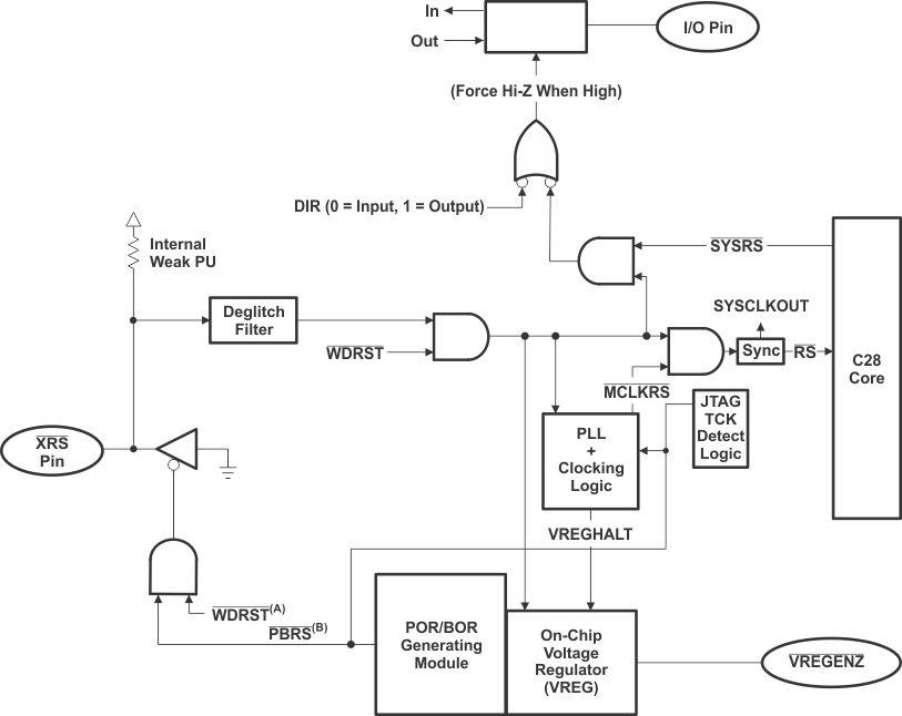
Two on-chip supervisory circuits, the power-on reset (POR) and the brown-out reset (BOR) remove the burden of monitoring the VDD and VDDIO supply rails from the application board. The purpose of the POR is to create a clean reset throughout the device during the entire power-up procedure. The trip point is a looser, lower trip point than the BOR, which watches for dips in the VDD or VDDIO rail during device operation. The POR function is present on both VDD and VDDIO rails at all times. After initial device power-up, the BOR function is present on VDDIO at all times, and on VDD when the internal VREG is enabled (VREGENZ pin is tied low). Both functions tie the XRS pin low when one of the voltages is below their respective trip point. VDD BOR and overvoltage trip points are outside of the recommended operating voltages. Proper device operation cannot be ensured. If overvoltage or undervoltage conditions affecting the system is a concern for an application, an external voltage supervisor should be added. Figure 5-2 shows the VREG, POR, and BOR. To disable both the VDD and VDDIO BOR functions, a bit is provided in the BORCFG register. For details, see the TMS320F2803x Piccolo System Control and Interrupts Reference Guide.
