ZHCSAH6F November 2012 – September 2021 TMS320F28050 , TMS320F28051 , TMS320F28052 , TMS320F28052F , TMS320F28052M , TMS320F28053 , TMS320F28054 , TMS320F28054F , TMS320F28054M , TMS320F28055
PRODUCTION DATA
- 1 特性
- 2 应用
- 3 说明
- 4 Revision History
- 5 Device Comparison
- 6 Terminal Configuration and Functions
-
7 Specifications
- 7.1 Absolute Maximum Ratings
- 7.2 ESD Ratings – Commercial
- 7.3 ESD Ratings – Automotive
- 7.4 Recommended Operating Conditions
- 7.5 Power Consumption Summary
- 7.6 Electrical Characteristics
- 7.7 Thermal Resistance Characteristics for PN Package
- 7.8 Thermal Design Considerations
- 7.9 JTAG Debug Probe Connection Without Signal Buffering for the MCU
- 7.10 Parameter Information
- 7.11 Test Load Circuit
- 7.12 Power Sequencing
- 7.13 Clock Specifications
- 7.14 Flash Timing
-
8 Detailed Description
- 8.1
Overview
- 8.1.1 CPU
- 8.1.2 Control Law Accelerator
- 8.1.3 Memory Bus (Harvard Bus Architecture)
- 8.1.4 Peripheral Bus
- 8.1.5 Real-Time JTAG and Analysis
- 8.1.6 Flash
- 8.1.7 M0, M1 SARAMs
- 8.1.8 L0 SARAM, and L1, L2, and L3 DPSARAMs
- 8.1.9 Boot ROM
- 8.1.10 Security
- 8.1.11 Peripheral Interrupt Expansion Block
- 8.1.12 External Interrupts (XINT1 to XINT3)
- 8.1.13 Internal Zero-Pin Oscillators, Oscillator, and PLL
- 8.1.14 Watchdog
- 8.1.15 Peripheral Clocking
- 8.1.16 Low-power Modes
- 8.1.17 Peripheral Frames 0, 1, 2, 3 (PFn)
- 8.1.18 General-Purpose Input/Output Multiplexer
- 8.1.19 32-Bit CPU-Timers (0, 1, 2)
- 8.1.20 Control Peripherals
- 8.1.21 Serial Port Peripherals
- 8.2 Memory Maps
- 8.3 Register Map
- 8.4 Device Emulation Registers
- 8.5 VREG, BOR, POR
- 8.6 System Control
- 8.7 Low-power Modes Block
- 8.8 Interrupts
- 8.9
Peripherals
- 8.9.1 Control Law Accelerator
- 8.9.2
Analog Block
- 8.9.2.1
Analog-to-Digital Converter
- 8.9.2.1.1 ADC Device-Specific Information
- 8.9.2.1.2 ADC Electrical Data/Timing
- 8.9.2.2 Analog Front End
- 8.9.2.1
Analog-to-Digital Converter
- 8.9.3 Detailed Descriptions
- 8.9.4 Serial Peripheral Interface
- 8.9.5 Serial Communications Interface
- 8.9.6 Enhanced Controller Area Network
- 8.9.7 Inter-Integrated Circuit
- 8.9.8 Enhanced Pulse Width Modulator
- 8.9.9 Enhanced Capture Module
- 8.9.10 Enhanced Quadrature Encoder Pulse
- 8.9.11 JTAG Port
- 8.9.12 General-Purpose Input/Output
- 8.1
Overview
- 9 Applications, Implementation, and Layout
- 10Device and Documentation Support
- 11Mechanical, Packaging, and Orderable Information
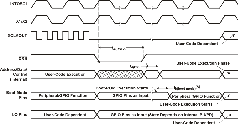
7.12.2 Reset ( XRS) Switching Characteristics
over recommended operating conditions (unless otherwise noted)
| PARAMETER | MIN | TYP | MAX | UNIT | |
|---|---|---|---|---|---|
| tw(RSL1) | Pulse duration, XRS driven by device | 600 | μs | ||
| tw(WDRS) | Pulse duration, reset pulse generated by watchdog | 512tc(OSCCLK) | cycles | ||
| td(EX) | Delay time, address/data valid after XRS high | 32tc(OSCCLK) | cycles | ||
| tINTOSCST | Start-up time, internal zero-pin oscillator | 3 | μs | ||
| tOSCST (1) | On-chip crystal-oscillator start-up time | 1 | 10 | ms | |
(1) Dependent on crystal/resonator and board design.

After reset, the Boot ROM code samples BOOT Mode pins. Based on the status of the Boot Mode pin, the boot code branches to destination memory or boot code function. If Boot ROM code executes after power-on conditions (in debugger environment), the Boot code execution time is based on the current SYSCLKOUT speed. The SYSCLKOUT will be based on user environment and could be with or without PLL enabled.
Figure 7-7 Warm ResetFigure 7-8 shows an example for the effect of writing into PLLCR register. In the first phase, PLLCR = 0x0004 and SYSCLKOUT = OSCCLK × 2. The PLLCR is then written with 0x0008. Immediately after the PLLCR register is written, the PLL lock-up phase begins. During this phase, SYSCLKOUT = OSCCLK/2. After the PLL lock-up is complete, SYSCLKOUT reflects the new operating frequency, OSCCLK × 4.
 Figure 7-8 Example of Effect of Writing Into PLLCR Register