ZHCSAH6F November 2012 – September 2021 TMS320F28050 , TMS320F28051 , TMS320F28052 , TMS320F28052F , TMS320F28052M , TMS320F28053 , TMS320F28054 , TMS320F28054F , TMS320F28054M , TMS320F28055
PRODUCTION DATA
- 1 特性
- 2 应用
- 3 说明
- 4 Revision History
- 5 Device Comparison
- 6 Terminal Configuration and Functions
-
7 Specifications
- 7.1 Absolute Maximum Ratings
- 7.2 ESD Ratings – Commercial
- 7.3 ESD Ratings – Automotive
- 7.4 Recommended Operating Conditions
- 7.5 Power Consumption Summary
- 7.6 Electrical Characteristics
- 7.7 Thermal Resistance Characteristics for PN Package
- 7.8 Thermal Design Considerations
- 7.9 JTAG Debug Probe Connection Without Signal Buffering for the MCU
- 7.10 Parameter Information
- 7.11 Test Load Circuit
- 7.12 Power Sequencing
- 7.13 Clock Specifications
- 7.14 Flash Timing
-
8 Detailed Description
- 8.1
Overview
- 8.1.1 CPU
- 8.1.2 Control Law Accelerator
- 8.1.3 Memory Bus (Harvard Bus Architecture)
- 8.1.4 Peripheral Bus
- 8.1.5 Real-Time JTAG and Analysis
- 8.1.6 Flash
- 8.1.7 M0, M1 SARAMs
- 8.1.8 L0 SARAM, and L1, L2, and L3 DPSARAMs
- 8.1.9 Boot ROM
- 8.1.10 Security
- 8.1.11 Peripheral Interrupt Expansion Block
- 8.1.12 External Interrupts (XINT1 to XINT3)
- 8.1.13 Internal Zero-Pin Oscillators, Oscillator, and PLL
- 8.1.14 Watchdog
- 8.1.15 Peripheral Clocking
- 8.1.16 Low-power Modes
- 8.1.17 Peripheral Frames 0, 1, 2, 3 (PFn)
- 8.1.18 General-Purpose Input/Output Multiplexer
- 8.1.19 32-Bit CPU-Timers (0, 1, 2)
- 8.1.20 Control Peripherals
- 8.1.21 Serial Port Peripherals
- 8.2 Memory Maps
- 8.3 Register Map
- 8.4 Device Emulation Registers
- 8.5 VREG, BOR, POR
- 8.6 System Control
- 8.7 Low-power Modes Block
- 8.8 Interrupts
- 8.9
Peripherals
- 8.9.1 Control Law Accelerator
- 8.9.2
Analog Block
- 8.9.2.1
Analog-to-Digital Converter
- 8.9.2.1.1 ADC Device-Specific Information
- 8.9.2.1.2 ADC Electrical Data/Timing
- 8.9.2.2 Analog Front End
- 8.9.2.1
Analog-to-Digital Converter
- 8.9.3 Detailed Descriptions
- 8.9.4 Serial Peripheral Interface
- 8.9.5 Serial Communications Interface
- 8.9.6 Enhanced Controller Area Network
- 8.9.7 Inter-Integrated Circuit
- 8.9.8 Enhanced Pulse Width Modulator
- 8.9.9 Enhanced Capture Module
- 8.9.10 Enhanced Quadrature Encoder Pulse
- 8.9.11 JTAG Port
- 8.9.12 General-Purpose Input/Output
- 8.1
Overview
- 9 Applications, Implementation, and Layout
- 10Device and Documentation Support
- 11Mechanical, Packaging, and Orderable Information
8.8 Interrupts
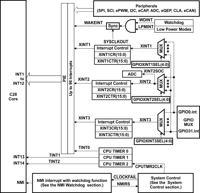
Figure 8-12 shows how the various interrupt sources are multiplexed.
 Figure 8-12 External and PIE Interrupt Sources
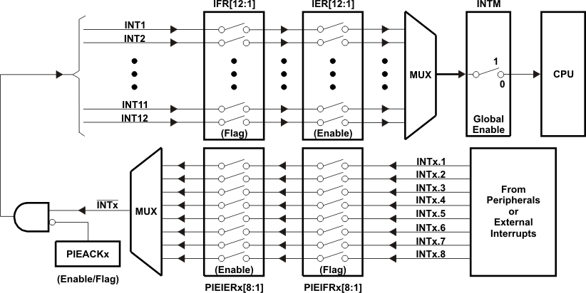
Eight PIE block interrupts are grouped into one CPU interrupt. In total, 12 CPU interrupt groups, with 8 interrupts per group equals 96 possible interrupts. Table 8-23 shows the interrupts used by 2805x devices.
The TRAP #VectorNumber instruction transfers program control to the interrupt service routine (ISR) corresponding to the vector specified. TRAP #0 attempts to transfer program control to the address pointed to by the reset vector. The PIE vector table does not, however, include a reset vector. Therefore, TRAP #0 should not be used when the PIE is enabled. Doing so will result in undefined behavior.
When the PIE is enabled, TRAP #1 to TRAP #12 will transfer program control to the ISR corresponding to the first vector within the PIE group. For example: TRAP #1 fetches the vector from INT1.1, TRAP #2 fetches the vector from INT2.1, and so forth.
 Figure 8-13 Multiplexing of Interrupts Using the PIE Block
In Table 8-23, out of 96 possible interrupts, some interrupts are not used. These interrupts are reserved for future devices. These interrupts can be used as software interrupts if they are enabled at the PIEIFRx level, provided none of the interrupts within the group is being used by a peripheral. Otherwise, interrupts coming in from peripherals may be lost by accidentally clearing their flag while modifying the PIEIFR. To summarize, there are two safe cases when the reserved interrupts could be used as software interrupts:
- No peripheral within the group is asserting interrupts.
- No peripheral interrupts are assigned to the group (for example, PIE group 7).
| INTx.8 | INTx.7 | INTx.6 | INTx.5 | INTx.4 | INTx.3 | INTx.2 | INTx.1 | |
|---|---|---|---|---|---|---|---|---|
| INT1.y | WAKEINT | TINT0 | ADCINT9 | XINT2 | XINT1 | Reserved | ADCINT2 | ADCINT1 |
| (LPM/WD) | (TIMER 0) | (ADC) | Ext. int. 2 | Ext. int. 1 | – | (ADC) | (ADC) | |
| 0xD4E | 0xD4C | 0xD4A | 0xD48 | 0xD46 | 0xD44 | 0xD42 | 0xD40 | |
| INT2.y | Reserved | EPWM7_TZINT | EPWM6_TZINT | EPWM5_TZINT | EPWM4_TZINT | EPWM3_TZINT | EPWM2_TZINT | EPWM1_TZINT |
| – | (ePWM7) | (ePWM6) | (ePWM5) | (ePWM4) | (ePWM3) | (ePWM2) | (ePWM1) | |
| 0xD5E | 0xD5C | 0xD5A | 0xD58 | 0xD56 | 0xD54 | 0xD52 | 0xD50 | |
| INT3.y | Reserved | EPWM7_INT | EPWM6_INT | EPWM5_INT | EPWM4_INT | EPWM3_INT | EPWM2_INT | EPWM1_INT |
| – | (ePWM7) | (ePWM6) | (ePWM5) | (ePWM4) | (ePWM3) | (ePWM2) | (ePWM1) | |
| 0xD6E | 0xD6C | 0xD6A | 0xD68 | 0xD66 | 0xD64 | 0xD62 | 0xD60 | |
| INT4.y | Reserved | Reserved | Reserved | Reserved | Reserved | Reserved | Reserved | ECAP1_INT |
| – | – | – | – | – | – | – | (eCAP1) | |
| 0xD7E | 0xD7C | 0xD7A | 0xD78 | 0xD76 | 0xD74 | 0xD72 | 0xD70 | |
| INT5.y | Reserved | Reserved | Reserved | Reserved | Reserved | Reserved | Reserved | EQEP1_INT |
| – | – | – | – | – | – | – | (eQEP1) | |
| 0xD8E | 0xD8C | 0xD8A | 0xD88 | 0xD86 | 0xD84 | 0xD82 | 0xD80 | |
| INT6.y | Reserved | Reserved | Reserved | Reserved | Reserved | Reserved | SPITXINTA | SPIRXINTA |
| – | – | – | – | – | – | (SPI-A) | (SPI-A) | |
| 0xD9E | 0xD9C | 0xD9A | 0xD98 | 0xD96 | 0xD94 | 0xD92 | 0xD90 | |
| INT7.y | Reserved | Reserved | Reserved | Reserved | Reserved | Reserved | Reserved | Reserved |
| – | – | – | – | – | – | – | – | |
| 0xDAE | 0xDAC | 0xDAA | 0xDA8 | 0xDA6 | 0xDA4 | 0xDA2 | 0xDA0 | |
| INT8.y | Reserved | Reserved | SCITXINTC | SCIRXINTC | Reserved | Reserved | I2CINT2A | I2CINT1A |
| – | – | (SCI-C) | (SCI-C) | – | – | (I2C-A) | (I2C-A) | |
| 0xDBE | 0xDBC | 0xDBA | 0xDB8 | 0xDB6 | 0xDB4 | 0xDB2 | 0xDB0 | |
| INT9.y | Reserved | Reserved | ECAN1_INTA | ECAN0_INTA | SCITXINTB | SCIRXINTB | SCITXINTA | SCIRXINTA |
| – | – | (CAN-A) | (CAN-A) | (SCI-B) | (SCI-B) | (SCI-A) | (SCI-A) | |
| 0xDCE | 0xDCC | 0xDCA | 0xDC8 | 0xDC6 | 0xDC4 | 0xDC2 | 0xDC0 | |
| INT10.y | ADCINT8 | ADCINT7 | ADCINT6 | ADCINT5 | ADCINT4 | ADCINT3 | ADCINT2 | ADCINT1 |
| (ADC) | (ADC) | (ADC) | (ADC) | (ADC) | (ADC) | (ADC) | (ADC) | |
| (ePWM16) | (ePWM15) | (ePWM14) | (ePWM13) | (ePWM12) | (ePWM11) | (ePWM10) | (ePWM9) | |
| 0xDDE | 0xDDC | 0xDDA | 0xDD8 | 0xDD6 | 0xDD4 | 0xDD2 | 0xDD0 | |
| INT11.y | CLA1_INT8 | CLA1_INT7 | CLA1_INT6 | CLA1_INT5 | CLA1_INT4 | CLA1_INT3 | CLA1_INT2 | CLA1_INT1 |
| (CLA) | (CLA) | (CLA) | (CLA) | (CLA) | (CLA) | (CLA) | (CLA) | |
| (ePWM16) | (ePWM15) | (ePWM14) | (ePWM13) | (ePWM12) | (ePWM11) | (ePWM10) | (ePWM9) | |
| 0xDEE | 0xDEC | 0xDEA | 0xDE8 | 0xDE6 | 0xDE4 | 0xDE2 | 0xDE0 | |
| INT12.y | LUF | LVF | Reserved | Reserved | Reserved | Reserved | Reserved | XINT3 |
| (CLA) | (CLA) | – | – | – | – | – | Ext. Int. 3 | |
| 0xDFE | 0xDFC | 0xDFA | 0xDF8 | 0xDF6 | 0xDF4 | 0xDF2 | 0xDF0 |
| NAME | ADDRESS | SIZE (×16) | DESCRIPTION(1) |
|---|---|---|---|
| PIECTRL | 0x0CE0 | 1 | PIE, Control register |
| PIEACK | 0x0CE1 | 1 | PIE, Acknowledge register |
| PIEIER1 | 0x0CE2 | 1 | PIE, INT1 Group Enable register |
| PIEIFR1 | 0x0CE3 | 1 | PIE, INT1 Group Flag register |
| PIEIER2 | 0x0CE4 | 1 | PIE, INT2 Group Enable register |
| PIEIFR2 | 0x0CE5 | 1 | PIE, INT2 Group Flag register |
| PIEIER3 | 0x0CE6 | 1 | PIE, INT3 Group Enable register |
| PIEIFR3 | 0x0CE7 | 1 | PIE, INT3 Group Flag register |
| PIEIER4 | 0x0CE8 | 1 | PIE, INT4 Group Enable register |
| PIEIFR4 | 0x0CE9 | 1 | PIE, INT4 Group Flag register |
| PIEIER5 | 0x0CEA | 1 | PIE, INT5 Group Enable register |
| PIEIFR5 | 0x0CEB | 1 | PIE, INT5 Group Flag register |
| PIEIER6 | 0x0CEC | 1 | PIE, INT6 Group Enable register |
| PIEIFR6 | 0x0CED | 1 | PIE, INT6 Group Flag register |
| PIEIER7 | 0x0CEE | 1 | PIE, INT7 Group Enable register |
| PIEIFR7 | 0x0CEF | 1 | PIE, INT7 Group Flag register |
| PIEIER8 | 0x0CF0 | 1 | PIE, INT8 Group Enable register |
| PIEIFR8 | 0x0CF1 | 1 | PIE, INT8 Group Flag register |
| PIEIER9 | 0x0CF2 | 1 | PIE, INT9 Group Enable register |
| PIEIFR9 | 0x0CF3 | 1 | PIE, INT9 Group Flag register |
| PIEIER10 | 0x0CF4 | 1 | PIE, INT10 Group Enable register |
| PIEIFR10 | 0x0CF5 | 1 | PIE, INT10 Group Flag register |
| PIEIER11 | 0x0CF6 | 1 | PIE, INT11 Group Enable register |
| PIEIFR11 | 0x0CF7 | 1 | PIE, INT11 Group Flag register |
| PIEIER12 | 0x0CF8 | 1 | PIE, INT12 Group Enable register |
| PIEIFR12 | 0x0CF9 | 1 | PIE, INT12 Group Flag register |
| Reserved | 0x0CFA – 0x0CFF | 6 | Reserved |