ZHCSAH6F November 2012 – September 2021 TMS320F28050 , TMS320F28051 , TMS320F28052 , TMS320F28052F , TMS320F28052M , TMS320F28053 , TMS320F28054 , TMS320F28054F , TMS320F28054M , TMS320F28055
PRODUCTION DATA
- 1 特性
- 2 应用
- 3 说明
- 4 Revision History
- 5 Device Comparison
- 6 Terminal Configuration and Functions
-
7 Specifications
- 7.1 Absolute Maximum Ratings
- 7.2 ESD Ratings – Commercial
- 7.3 ESD Ratings – Automotive
- 7.4 Recommended Operating Conditions
- 7.5 Power Consumption Summary
- 7.6 Electrical Characteristics
- 7.7 Thermal Resistance Characteristics for PN Package
- 7.8 Thermal Design Considerations
- 7.9 JTAG Debug Probe Connection Without Signal Buffering for the MCU
- 7.10 Parameter Information
- 7.11 Test Load Circuit
- 7.12 Power Sequencing
- 7.13 Clock Specifications
- 7.14 Flash Timing
-
8 Detailed Description
- 8.1
Overview
- 8.1.1 CPU
- 8.1.2 Control Law Accelerator
- 8.1.3 Memory Bus (Harvard Bus Architecture)
- 8.1.4 Peripheral Bus
- 8.1.5 Real-Time JTAG and Analysis
- 8.1.6 Flash
- 8.1.7 M0, M1 SARAMs
- 8.1.8 L0 SARAM, and L1, L2, and L3 DPSARAMs
- 8.1.9 Boot ROM
- 8.1.10 Security
- 8.1.11 Peripheral Interrupt Expansion Block
- 8.1.12 External Interrupts (XINT1 to XINT3)
- 8.1.13 Internal Zero-Pin Oscillators, Oscillator, and PLL
- 8.1.14 Watchdog
- 8.1.15 Peripheral Clocking
- 8.1.16 Low-power Modes
- 8.1.17 Peripheral Frames 0, 1, 2, 3 (PFn)
- 8.1.18 General-Purpose Input/Output Multiplexer
- 8.1.19 32-Bit CPU-Timers (0, 1, 2)
- 8.1.20 Control Peripherals
- 8.1.21 Serial Port Peripherals
- 8.2 Memory Maps
- 8.3 Register Map
- 8.4 Device Emulation Registers
- 8.5 VREG, BOR, POR
- 8.6 System Control
- 8.7 Low-power Modes Block
- 8.8 Interrupts
- 8.9
Peripherals
- 8.9.1 Control Law Accelerator
- 8.9.2
Analog Block
- 8.9.2.1
Analog-to-Digital Converter
- 8.9.2.1.1 ADC Device-Specific Information
- 8.9.2.1.2 ADC Electrical Data/Timing
- 8.9.2.2 Analog Front End
- 8.9.2.1
Analog-to-Digital Converter
- 8.9.3 Detailed Descriptions
- 8.9.4 Serial Peripheral Interface
- 8.9.5 Serial Communications Interface
- 8.9.6 Enhanced Controller Area Network
- 8.9.7 Inter-Integrated Circuit
- 8.9.8 Enhanced Pulse Width Modulator
- 8.9.9 Enhanced Capture Module
- 8.9.10 Enhanced Quadrature Encoder Pulse
- 8.9.11 JTAG Port
- 8.9.12 General-Purpose Input/Output
- 8.1
Overview
- 9 Applications, Implementation, and Layout
- 10Device and Documentation Support
- 11Mechanical, Packaging, and Orderable Information
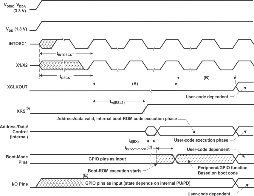
7.12 Power Sequencing
There is no power sequencing requirement needed to ensure the device is in the proper state after reset or to prevent the I/Os from glitching during power up or power down (GPIO19, GPIO34 to GPIO38 do not have glitch-free I/Os). No voltage larger than a diode drop (0.7 V) above VDDIO should be applied to any digital pin (for analog pins, this value is 0.7 V above VDDA) before powering up the device. Voltages applied to pins on an unpowered device can bias internal p-n junctions in unintended ways and produce unpredictable results.
