ZHCSAH6F November 2012 – September 2021 TMS320F28050 , TMS320F28051 , TMS320F28052 , TMS320F28052F , TMS320F28052M , TMS320F28053 , TMS320F28054 , TMS320F28054F , TMS320F28054M , TMS320F28055
PRODUCTION DATA
- 1 特性
- 2 应用
- 3 说明
- 4 Revision History
- 5 Device Comparison
- 6 Terminal Configuration and Functions
-
7 Specifications
- 7.1 Absolute Maximum Ratings
- 7.2 ESD Ratings – Commercial
- 7.3 ESD Ratings – Automotive
- 7.4 Recommended Operating Conditions
- 7.5 Power Consumption Summary
- 7.6 Electrical Characteristics
- 7.7 Thermal Resistance Characteristics for PN Package
- 7.8 Thermal Design Considerations
- 7.9 JTAG Debug Probe Connection Without Signal Buffering for the MCU
- 7.10 Parameter Information
- 7.11 Test Load Circuit
- 7.12 Power Sequencing
- 7.13 Clock Specifications
- 7.14 Flash Timing
-
8 Detailed Description
- 8.1
Overview
- 8.1.1 CPU
- 8.1.2 Control Law Accelerator
- 8.1.3 Memory Bus (Harvard Bus Architecture)
- 8.1.4 Peripheral Bus
- 8.1.5 Real-Time JTAG and Analysis
- 8.1.6 Flash
- 8.1.7 M0, M1 SARAMs
- 8.1.8 L0 SARAM, and L1, L2, and L3 DPSARAMs
- 8.1.9 Boot ROM
- 8.1.10 Security
- 8.1.11 Peripheral Interrupt Expansion Block
- 8.1.12 External Interrupts (XINT1 to XINT3)
- 8.1.13 Internal Zero-Pin Oscillators, Oscillator, and PLL
- 8.1.14 Watchdog
- 8.1.15 Peripheral Clocking
- 8.1.16 Low-power Modes
- 8.1.17 Peripheral Frames 0, 1, 2, 3 (PFn)
- 8.1.18 General-Purpose Input/Output Multiplexer
- 8.1.19 32-Bit CPU-Timers (0, 1, 2)
- 8.1.20 Control Peripherals
- 8.1.21 Serial Port Peripherals
- 8.2 Memory Maps
- 8.3 Register Map
- 8.4 Device Emulation Registers
- 8.5 VREG, BOR, POR
- 8.6 System Control
- 8.7 Low-power Modes Block
- 8.8 Interrupts
- 8.9
Peripherals
- 8.9.1 Control Law Accelerator
- 8.9.2
Analog Block
- 8.9.2.1
Analog-to-Digital Converter
- 8.9.2.1.1 ADC Device-Specific Information
- 8.9.2.1.2 ADC Electrical Data/Timing
- 8.9.2.2 Analog Front End
- 8.9.2.1
Analog-to-Digital Converter
- 8.9.3 Detailed Descriptions
- 8.9.4 Serial Peripheral Interface
- 8.9.5 Serial Communications Interface
- 8.9.6 Enhanced Controller Area Network
- 8.9.7 Inter-Integrated Circuit
- 8.9.8 Enhanced Pulse Width Modulator
- 8.9.9 Enhanced Capture Module
- 8.9.10 Enhanced Quadrature Encoder Pulse
- 8.9.11 JTAG Port
- 8.9.12 General-Purpose Input/Output
- 8.1
Overview
- 9 Applications, Implementation, and Layout
- 10Device and Documentation Support
- 11Mechanical, Packaging, and Orderable Information
8.5.2 On-chip Power-On Reset and Brownout Reset Circuit
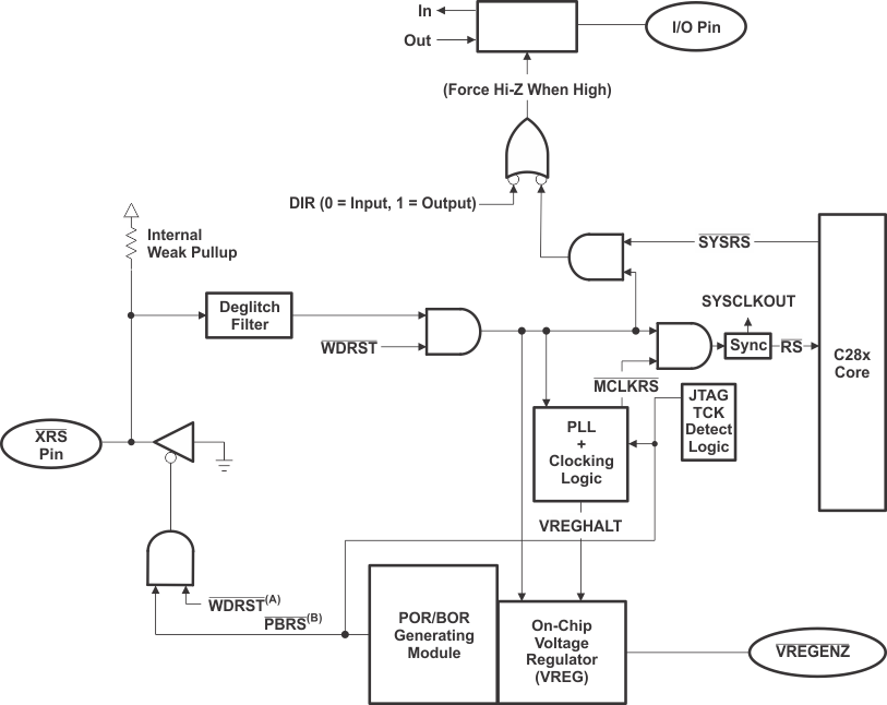
The purpose of the POR is to create a clean reset throughout the device during the entire power-up procedure. The trip point is a looser, lower trip point than the BOR, which watches for dips in the VDD or VDDIO rail during device operation. The POR function is present on both VDD and VDDIO rails at all times. After initial device power-up, the BOR function is present on VDDIO at all times, and on VDD when the internal VREG is enabled ( VREGENZ pin is tied low). Both functions tie the XRS pin low when one of the voltages is below its respective trip point. Additionally, when the internal voltage regulator is enabled, an overvoltage protection circuit will tie XRS low if the VDD rail rises above its trip point. See Section 7.6 for the various trip points as well as the delay time for the device to release the XRS pin after the undervoltage or overvoltage condition is removed. Figure 8-5 shows the VREG, POR, and BOR. To disable both the VDD and VDDIO BOR functions, a bit is provided in the BORCFG register. For details, see the System Control and Interrupts chapter of the TMS320x2805x Real-Time Microcontrollers Technical Reference Manual.
