ZHCS898O October   2003  – March 2019 TMS320F2801 , TMS320F28015 , TMS320F28016 , TMS320F2802 , TMS320F2806 , TMS320F2808 , TMS320F2809

PRODUCTION DATA.  

  1. 1器件概述
    1. 1.1 特性
    2. 1.2 应用
    3. 1.3 说明
    4. 1.4 功能方框图
  2. 2修订历史记录
  3. 3Device Comparison
    1. 3.1 Related Products
  4. 4Terminal Configuration and Functions
    1. 4.1 Pin Diagrams
    2. 4.2 Signal Descriptions
  5. 5Specifications
    1. 5.1  Absolute Maximum Ratings
    2. 5.2  ESD Ratings – Automotive
    3. 5.3  ESD Ratings – Commercial
    4. 5.4  Recommended Operating Conditions
    5. 5.5  Power Consumption Summary
      1. Table 5-1 TMS320F2809, TMS320F2808 Current Consumption by Power-Supply Pins at 100-MHz SYSCLKOUT
      2. Table 5-2 TMS320F2806 Current Consumption by Power-Supply Pins at 100-MHz SYSCLKOUT
      3. Table 5-3 TMS320F2802, TMS320F2801 Current Consumption by Power-Supply Pins at 100-MHz SYSCLKOUT
      4. Table 5-4 TMS320C2802, TMS320C2801 Current Consumption by Power-Supply Pins at 100-MHz SYSCLKOUT
      5. 5.5.1     Reducing Current Consumption
      6. 5.5.2     Current Consumption Graphs
    6. 5.6  Electrical Characteristics
    7. 5.7  Thermal Resistance Characteristics for F280x 100-Ball GGM Package
    8. 5.8  Thermal Resistance Characteristics for F280x 100-Pin PZ Package
    9. 5.9  Thermal Resistance Characteristics for C280x 100-Ball GGM Package
    10. 5.10 Thermal Resistance Characteristics for C280x 100-Pin PZ Package
    11. 5.11 Thermal Resistance Characteristics for F2809 100-Ball GGM Package
    12. 5.12 Thermal Resistance Characteristics for F2809 100-Pin PZ Package
    13. 5.13 Thermal Design Considerations
    14. 5.14 Timing and Switching Characteristics
      1. 5.14.1 Timing Parameter Symbology
        1. 5.14.1.1 General Notes on Timing Parameters
        2. 5.14.1.2 Test Load Circuit
        3. 5.14.1.3 Device Clock Table
          1. Table 5-6 TMS320x280x Clock Table and Nomenclature (100-MHz Devices)
          2. Table 5-7 TMS320x280x/2801x Clock Table and Nomenclature (60-MHz Devices)
      2. 5.14.2 Power Sequencing
        1. Table 5-8 Reset (XRS) Timing Requirements
      3. 5.14.3 Clock Requirements and Characteristics
        1. Table 5-9  Input Clock Frequency
        2. Table 5-10 XCLKIN Timing Requirements - PLL Enabled
        3. Table 5-11 XCLKIN Timing Requirements - PLL Disabled
        4. Table 5-12 XCLKOUT Switching Characteristics (PLL Bypassed or Enabled)
      4. 5.14.4 Peripherals
        1. 5.14.4.1 General-Purpose Input/Output (GPIO)
          1. 5.14.4.1.1 GPIO - Output Timing
            1. Table 5-13 General-Purpose Output Switching Characteristics
          2. 5.14.4.1.2 GPIO - Input Timing
            1. Table 5-14 General-Purpose Input Timing Requirements
          3. 5.14.4.1.3 Sampling Window Width for Input Signals
          4. 5.14.4.1.4 Low-Power Mode Wakeup Timing
            1. Table 5-15 IDLE Mode Timing Requirements
            2. Table 5-16 IDLE Mode Switching Characteristics
            3. Table 5-17 STANDBY Mode Timing Requirements
            4. Table 5-18 STANDBY Mode Switching Characteristics
            5. Table 5-19 HALT Mode Timing Requirements
            6. Table 5-20 HALT Mode Switching Characteristics
        2. 5.14.4.2 Enhanced Control Peripherals
          1. 5.14.4.2.1 Enhanced Pulse Width Modulator (ePWM) Timing
            1. Table 5-21 ePWM Timing Requirements
            2. Table 5-22 ePWM Switching Characteristics
          2. 5.14.4.2.2 Trip-Zone Input Timing
            1. Table 5-23 Trip-Zone input Timing Requirements
          3. 5.14.4.2.3 High-Resolution PWM Timing
            1. Table 5-24 High-Resolution PWM Characteristics at SYSCLKOUT = 60–100 MHz
          4. 5.14.4.2.4 Enhanced Capture (eCAP) Timing
            1. Table 5-25 Enhanced Capture (eCAP) Timing Requirement
            2. Table 5-26 eCAP Switching Characteristics
          5. 5.14.4.2.5 Enhanced Quadrature Encoder Pulse (eQEP) Timing
            1. Table 5-27 Enhanced Quadrature Encoder Pulse (eQEP) Timing Requirements
            2. Table 5-28 eQEP Switching Characteristics
          6. 5.14.4.2.6 ADC Start-of-Conversion Timing
            1. Table 5-29 External ADC Start-of-Conversion Switching Characteristics
        3. 5.14.4.3 External Interrupt Timing
          1. Table 5-30 External Interrupt Timing Requirements
          2. Table 5-31 External Interrupt Switching Characteristics
        4. 5.14.4.4 I2C Electrical Specification and Timing
          1. Table 5-32 I2C Timing
        5. 5.14.4.5 Serial Peripheral Interface (SPI) Timing
          1. 5.14.4.5.1 SPI Master Mode Timing
            1. Table 5-33 SPI Master Mode External Timing (Clock Phase = 0)
            2. Table 5-34 SPI Master Mode External Timing (Clock Phase = 1)
          2. 5.14.4.5.2 SPI Slave Mode Timing
            1. Table 5-35 SPI Slave Mode External Timing (Clock Phase = 0)
            2. Table 5-36 SPI Slave Mode External Timing (Clock Phase = 1)
      5. 5.14.5 Emulator Connection Without Signal Buffering for the DSP
      6. 5.14.6 Flash Timing
        1. Table 5-37 Flash Endurance for A and S Temperature Material
        2. Table 5-38 Flash Endurance for Q Temperature Material
        3. Table 5-39 Flash Parameters at 100-MHz SYSCLKOUT
        4. Table 5-40 Flash/OTP Access Timing
        5. Table 5-41 Flash Data Retention Duration
    15. 5.15 On-Chip Analog-to-Digital Converter
      1. Table 5-43 ADC Electrical Characteristics
      2. 5.15.1     ADC Power-Up Control Bit Timing
        1. Table 5-44 ADC Power-Up Delays
        2. Table 5-45 Current Consumption for Different ADC Configurations (at 12.5-MHz ADCCLK)
      3. 5.15.2     Definitions
      4. 5.15.3     Sequential Sampling Mode (Single-Channel) (SMODE = 0)
        1. Table 5-46 Sequential Sampling Mode Timing
      5. 5.15.4     Simultaneous Sampling Mode (Dual-Channel) (SMODE = 1)
        1. Table 5-47 Simultaneous Sampling Mode Timing
      6. 5.15.5     Detailed Descriptions
    16. 5.16 Migrating From F280x Devices to C280x Devices
      1. 5.16.1 Migration Issues
    17. 5.17 ROM Timing (C280x only)
      1. Table 5-48 ROM/OTP Access Timing
  6. 6Detailed Description
    1. 6.1 Brief Descriptions
      1. 6.1.1  C28x CPU
      2. 6.1.2  Memory Bus (Harvard Bus Architecture)
      3. 6.1.3  Peripheral Bus
      4. 6.1.4  Real-Time JTAG and Analysis
      5. 6.1.5  Flash
      6. 6.1.6  ROM
      7. 6.1.7  M0, M1 SARAMs
      8. 6.1.8  L0, L1, H0 SARAMs
      9. 6.1.9  Boot ROM
      10. 6.1.10 Security
      11. 6.1.11 Peripheral Interrupt Expansion (PIE) Block
      12. 6.1.12 External Interrupts (XINT1, XINT2, XNMI)
      13. 6.1.13 Oscillator and PLL
      14. 6.1.14 Watchdog
      15. 6.1.15 Peripheral Clocking
      16. 6.1.16 Low-Power Modes
      17. 6.1.17 Peripheral Frames 0, 1, 2 (PFn)
      18. 6.1.18 General-Purpose Input/Output (GPIO) Multiplexer
      19. 6.1.19 32-Bit CPU-Timers (0, 1, 2)
      20. 6.1.20 Control Peripherals
      21. 6.1.21 Serial Port Peripherals
    2. 6.2 Peripherals
      1. 6.2.1  32-Bit CPU-Timers 0/1/2
      2. 6.2.2  Enhanced PWM Modules (ePWM1/2/3/4/5/6)
      3. 6.2.3  Hi-Resolution PWM (HRPWM)
      4. 6.2.4  Enhanced CAP Modules (eCAP1/2/3/4)
      5. 6.2.5  Enhanced QEP Modules (eQEP1/2)
      6. 6.2.6  Enhanced Analog-to-Digital Converter (ADC) Module
        1. 6.2.6.1 ADC Connections if the ADC Is Not Used
        2. 6.2.6.2 ADC Registers
      7. 6.2.7  Enhanced Controller Area Network (eCAN) Modules (eCAN-A and eCAN-B)
      8. 6.2.8  Serial Communications Interface (SCI) Modules (SCI-A, SCI-B)
      9. 6.2.9  Serial Peripheral Interface (SPI) Modules (SPI-A, SPI-B, SPI-C, SPI-D)
      10. 6.2.10 Inter-Integrated Circuit (I2C)
      11. 6.2.11 GPIO MUX
    3. 6.3 Memory Maps
    4. 6.4 Register Map
      1. 6.4.1 Device Emulation Registers
    5. 6.5 Interrupts
      1. 6.5.1 External Interrupts
    6. 6.6 System Control
      1. 6.6.1 OSC and PLL Block
        1. 6.6.1.1 External Reference Oscillator Clock Option
        2. 6.6.1.2 PLL-Based Clock Module
        3. 6.6.1.3 Loss of Input Clock
      2. 6.6.2 Watchdog Block
    7. 6.7 Low-Power Modes Block
  7. 7Applications, Implementation, and Layout
    1. 7.1 TI Design or Reference Design
  8. 8器件和文档支持
    1. 8.1 开始使用
    2. 8.2 器件和开发支持工具命名规则
    3. 8.3 工具与软件
    4. 8.4 文档支持
    5. 8.5 相关链接
    6. 8.6 Community Resources
    7. 8.7 商标
    8. 8.8 静电放电警告
    9. 8.9 Glossary
  9. 9机械、封装和可订购信息
    1. 9.1 封装信息

封装选项

请参考 PDF 数据表获取器件具体的封装图。

机械数据 (封装 | 引脚)
  • PZ|100
  • NMF|100
散热焊盘机械数据 (封装 | 引脚)
订购信息

Table 5-18 STANDBY Mode Switching Characteristics

PARAMETER TEST CONDITIONS MIN MAX UNIT
td(IDLE-XCOL) Delay time, IDLE instruction executed to XCLKOUT low 32tc(SCO) 45tc(SCO) cycles
td(WAKE-STBY) Delay time, external wake signal to program execution resume(1)
  • Wake up from flash
    • Flash module in active state
Without input qualifier 100tc(SCO) cycles
With input qualifier 100tc(SCO) + tw(WAKE-INT)
  • Wake up from flash
    • Flash module in sleep state
Without input qualifier 1125tc(SCO) cycles
With input qualifier 1125tc(SCO) + tw(WAKE-INT)
  • Wake up from SARAM
Without input qualifier 100tc(SCO) cycles
With input qualifier 100tc(SCO) + tw(WAKE-INT)
This is the time taken to begin execution of the instruction that immediately follows the IDLE instruction. execution of an ISR (triggered by the wake up signal) involves additional latency.
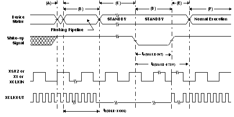
TMS320F2809 TMS320F2808 TMS320F2806 TMS320F2802 TMS320F2801 TMS320C2802 TMS320C2801 TMS320F28016 TMS320F28015 td_stdb_ex_prs230.gif
IDLE instruction is executed to put the device into STANDBY mode.
The PLL block responds to the STANDBY signal. SYSCLKOUT is held for approximately 32 cycles (if CLKINDIV = 0) or 64 cycles (if CLKINDIV = 1) before being turned off. This delay enables the CPU pipe and any other pending operations to flush properly.
Clock to the peripherals are turned off. However, the PLL and watchdog are not shut down. The device is now in STANDBY mode.
The external wake-up signal is driven active.
After a latency period, the STANDBY mode is exited.
Normal execution resumes. The device will respond to the interrupt (if enabled).
Figure 5-14 STANDBY Entry and Exit Timing Diagram