ZHCS009J November 2010 – September 2021 TMS320F28062 , TMS320F28062F , TMS320F28063 , TMS320F28064 , TMS320F28065 , TMS320F28066 , TMS320F28067 , TMS320F28068F , TMS320F28068M , TMS320F28069 , TMS320F28069F , TMS320F28069M
PRODUCTION DATA
- 1 特性
- 2 应用
- 3 说明
- 4 Revision History
- 5 Device Comparison
- 6 Terminal Configuration and Functions
-
7 Specifications
- 7.1 Absolute Maximum Ratings
- 7.2 ESD Ratings – Commercial
- 7.3 ESD Ratings – Automotive
- 7.4 Recommended Operating Conditions
- 7.5 Power Consumption Summary
- 7.6 Electrical Characteristics
- 7.7 Thermal Resistance Characteristics
- 7.8 Thermal Design Considerations
- 7.9 Debug Probe Connection Without Signal Buffering for the MCU
- 7.10 Parameter Information
- 7.11 Test Load Circuit
- 7.12 Power Sequencing
- 7.13 Clock Specifications
- 7.14 Flash Timing
-
8 Detailed Description
- 8.1
Overview
- 8.1.1 CPU
- 8.1.2 Control Law Accelerator (CLA)
- 8.1.3 Viterbi, Complex Math, CRC Unit (VCU)
- 8.1.4 Memory Bus (Harvard Bus Architecture)
- 8.1.5 Peripheral Bus
- 8.1.6 Real-Time JTAG and Analysis
- 8.1.7 Flash
- 8.1.8 M0, M1 SARAMs
- 8.1.9 L4 SARAM, and L0, L1, L2, L3, L5, L6, L7, and L8 DPSARAMs
- 8.1.10 Boot ROM
- 8.1.11 Security
- 8.1.12 Peripheral Interrupt Expansion (PIE) Block
- 8.1.13 External Interrupts (XINT1 to XINT3)
- 8.1.14 Internal Zero Pin Oscillators, Oscillator, and PLL
- 8.1.15 Watchdog
- 8.1.16 Peripheral Clocking
- 8.1.17 Low-power Modes
- 8.1.18 Peripheral Frames 0, 1, 2, 3 (PFn)
- 8.1.19 General-Purpose Input/Output (GPIO) Multiplexer
- 8.1.20 32-Bit CPU-Timers (0, 1, 2)
- 8.1.21 Control Peripherals
- 8.1.22 Serial Port Peripherals
- 8.2 Memory Maps
- 8.3 Register Maps
- 8.4 Device Debug Registers
- 8.5 VREG, BOR, POR
- 8.6 System Control
- 8.7 Low-power Modes Block
- 8.8 Interrupts
- 8.9
Peripherals
- 8.9.1 CLA Overview
- 8.9.2 Analog Block
- 8.9.3 Detailed Descriptions
- 8.9.4 Serial Peripheral Interface (SPI) Module
- 8.9.5 Serial Communications Interface (SCI) Module
- 8.9.6
Multichannel Buffered Serial Port (McBSP) Module
- 8.9.6.1
McBSP Electrical Data/Timing
- 8.9.6.1.1 McBSP Transmit and Receive Timing
- 8.9.6.1.2
McBSP as SPI Master or Slave Timing
- 8.9.6.1.2.1 McBSP as SPI Master or Slave Timing Requirements (CLKSTP = 10b, CLKXP = 0)
- 8.9.6.1.2.2 McBSP as SPI Master or Slave Switching Characteristics (CLKSTP = 10b, CLKXP = 0)
- 8.9.6.1.2.3 McBSP as SPI Master or Slave Timing Requirements (CLKSTP = 11b, CLKXP = 0)
- 8.9.6.1.2.4 McBSP as SPI Master or Slave Switching Characteristics (CLKSTP = 11b, CLKXP = 0)
- 8.9.6.1.2.5 McBSP as SPI Master or Slave Timing Requirements (CLKSTP = 10b, CLKXP = 1)
- 8.9.6.1.2.6 McBSP as SPI Master or Slave Switching Characteristics (CLKSTP = 10b, CLKXP = 1)
- 8.9.6.1.2.7 McBSP as SPI Master or Slave Timing Requirements (CLKSTP = 11b, CLKXP = 1)
- 8.9.6.1.2.8 McBSP as SPI Master or Slave Switching Characteristics (CLKSTP = 11b, CLKXP = 1)
- 8.9.6.1
McBSP Electrical Data/Timing
- 8.9.7 Enhanced Controller Area Network (eCAN) Module
- 8.9.8 Inter-Integrated Circuit (I2C)
- 8.9.9 Enhanced Pulse Width Modulator (ePWM) Modules (ePWM1 to ePWM8)
- 8.9.10 High-Resolution PWM (HRPWM)
- 8.9.11 Enhanced Capture Module (eCAP1)
- 8.9.12 High-Resolution Capture Modules (HRCAP1 to HRCAP4)
- 8.9.13 Enhanced Quadrature Encoder Modules (eQEP1, eQEP2)
- 8.9.14 JTAG Port
- 8.9.15 General-Purpose Input/Output (GPIO) MUX
- 8.9.16 Universal Serial Bus (USB)
- 8.1
Overview
- 9 Applications, Implementation, and Layout
- 10Device and Documentation Support
- 11Mechanical, Packaging, and Orderable Information
封装选项
机械数据 (封装 | 引脚)
散热焊盘机械数据 (封装 | 引脚)
- PZ|100
订购信息
8.6 System Control
This section describes the oscillator and clocking mechanisms, the watchdog function and the low-power modes.
Table 8-11 PLL, Clocking, Watchdog, and Low-Power Mode Registers
| NAME | ADDRESS | SIZE (×16) | DESCRIPTION(1) |
|---|---|---|---|
| BORCFG | 0x00 0985 | 1 | BOR Configuration Register |
| XCLK | 0x00 7010 | 1 | XCLKOUT Control |
| PLLSTS | 0x00 7011 | 1 | PLL Status Register |
| CLKCTL | 0x00 7012 | 1 | Clock Control Register |
| PLLLOCKPRD | 0x00 7013 | 1 | PLL Lock Period |
| INTOSC1TRIM | 0x00 7014 | 1 | Internal Oscillator 1 Trim Register |
| INTOSC2TRIM | 0x00 7016 | 1 | Internal Oscillator 2 Trim Register |
| PCLKCR2 | 0x00 7019 | 1 | Peripheral Clock Control Register 2 |
| LOSPCP | 0x00 701B | 1 | Low-Speed Peripheral Clock Prescaler Register |
| PCLKCR0 | 0x00 701C | 1 | Peripheral Clock Control Register 0 |
| PCLKCR1 | 0x00 701D | 1 | Peripheral Clock Control Register 1 |
| LPMCR0 | 0x00 701E | 1 | Low-Power Mode Control Register 0 |
| PCLKCR3 | 0x00 7020 | 1 | Peripheral Clock Control Register 3 |
| PLLCR | 0x00 7021 | 1 | PLL Control Register |
| SCSR | 0x00 7022 | 1 | System Control and Status Register |
| WDCNTR | 0x00 7023 | 1 | Watchdog Counter Register |
| WDKEY | 0x00 7025 | 1 | Watchdog Reset Key Register |
| WDCR | 0x00 7029 | 1 | Watchdog Control Register |
| JTAGDEBUG | 0x00 702A | 1 | JTAG Port Debug Register |
| PLL2CTL | 0x00 7030 | 1 | PLL2 Configuration Register |
| PLL2MULT | 0x00 7032 | 1 | PLL2 Multiplier Register |
| PLL2STS | 0x00 7034 | 1 | PLL2 Lock Status Register |
| SYSCLK2CNTR | 0x00 7036 | 1 | SYSCLK2 Clock Counter Register |
| EPWMCFG | 0x00 703A | 1 | ePWM DMA/CLA Configuration Register |
(1) All registers in this table are EALLOW protected.
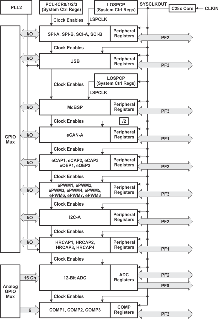
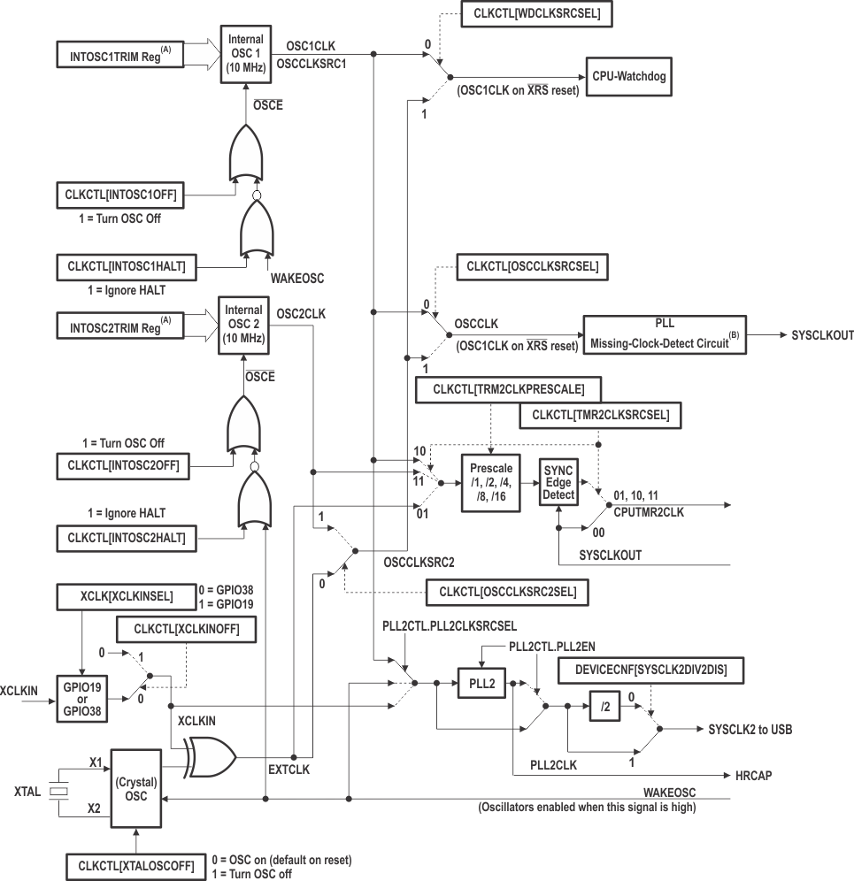
Figure 8-10 shows the various clock domains that are discussed. Figure 8-11 shows the various clock sources (both internal and external) that can provide a clock for device operation.

CLKIN is the clock into the CPU. CLKIN is passed out of the CPU as SYSCLKOUT (that is, CLKIN is the same frequency as SYSCLKOUT).
Figure 8-10 Clock and Reset Domains
Register loaded from TI OTP-based calibration function.
See Section 8.6.5 for details on missing clock detection.
Figure 8-11 Clock Tree