ZHCS009J November   2010  – September 2021 TMS320F28062 , TMS320F28062F , TMS320F28063 , TMS320F28064 , TMS320F28065 , TMS320F28066 , TMS320F28067 , TMS320F28068F , TMS320F28068M , TMS320F28069 , TMS320F28069F , TMS320F28069M

PRODUCTION DATA  

  1. 特性
  2. 应用
  3. 说明
    1. 3.1 功能方框图
    2. 3.2 系统器件图
  4. Revision History
  5. Device Comparison
    1. 5.1 Related Products
  6. Terminal Configuration and Functions
    1. 6.1 Pin Diagrams
    2. 6.2 Signal Descriptions
      1. 6.2.1 Signal Descriptions
  7. Specifications
    1. 7.1  Absolute Maximum Ratings
    2. 7.2  ESD Ratings – Commercial
    3. 7.3  ESD Ratings – Automotive
    4. 7.4  Recommended Operating Conditions
    5. 7.5  Power Consumption Summary
      1. 7.5.1 TMS320F2806x Current Consumption at 90-MHz SYSCLKOUT
      2. 7.5.2 Reducing Current Consumption
      3. 7.5.3 Current Consumption Graphs (VREG Enabled)
    6. 7.6  Electrical Characteristics
    7. 7.7  Thermal Resistance Characteristics
      1. 7.7.1 PFP PowerPAD Package
      2. 7.7.2 PZP PowerPAD Package
      3. 7.7.3 PN Package
      4. 7.7.4 PZ Package
    8. 7.8  Thermal Design Considerations
    9. 7.9  Debug Probe Connection Without Signal Buffering for the MCU
    10. 7.10 Parameter Information
      1. 7.10.1 Timing Parameter Symbology
      2. 7.10.2 General Notes on Timing Parameters
    11. 7.11 Test Load Circuit
    12. 7.12 Power Sequencing
      1. 7.12.1 Reset ( XRS) Timing Requirements
      2. 7.12.2 Reset ( XRS) Switching Characteristics
    13. 7.13 Clock Specifications
      1. 7.13.1 Device Clock Table
        1. 7.13.1.1 2806x Clock Table and Nomenclature (90-MHz Devices)
        2. 7.13.1.2 Device Clocking Requirements/Characteristics
        3. 7.13.1.3 Internal Zero-Pin Oscillator (INTOSC1/INTOSC2) Characteristics
      2. 7.13.2 Clock Requirements and Characteristics
        1. 7.13.2.1 XCLKIN Timing Requirements – PLL Enabled
        2. 7.13.2.2 XCLKIN Timing Requirements – PLL Disabled
        3. 7.13.2.3 XCLKOUT Switching Characteristics (PLL Bypassed or Enabled)
    14. 7.14 Flash Timing
      1. 7.14.1 Flash/OTP Endurance for T Temperature Material
      2. 7.14.2 Flash/OTP Endurance for S Temperature Material
      3. 7.14.3 Flash/OTP Endurance for Q Temperature Material
      4. 7.14.4 Flash Parameters at 90-MHz SYSCLKOUT
      5. 7.14.5 Flash/OTP Access Timing
      6. 7.14.6 Flash Data Retention Duration
  8. Detailed Description
    1. 8.1 Overview
      1. 8.1.1  CPU
      2. 8.1.2  Control Law Accelerator (CLA)
      3. 8.1.3  Viterbi, Complex Math, CRC Unit (VCU)
      4. 8.1.4  Memory Bus (Harvard Bus Architecture)
      5. 8.1.5  Peripheral Bus
      6. 8.1.6  Real-Time JTAG and Analysis
      7. 8.1.7  Flash
      8. 8.1.8  M0, M1 SARAMs
      9. 8.1.9  L4 SARAM, and L0, L1, L2, L3, L5, L6, L7, and L8 DPSARAMs
      10. 8.1.10 Boot ROM
        1. 8.1.10.1 Debug Boot
        2. 8.1.10.2 GetMode
        3. 8.1.10.3 Peripheral Pins Used by the Bootloader
      11. 8.1.11 Security
      12. 8.1.12 Peripheral Interrupt Expansion (PIE) Block
      13. 8.1.13 External Interrupts (XINT1 to XINT3)
      14. 8.1.14 Internal Zero Pin Oscillators, Oscillator, and PLL
      15. 8.1.15 Watchdog
      16. 8.1.16 Peripheral Clocking
      17. 8.1.17 Low-power Modes
      18. 8.1.18 Peripheral Frames 0, 1, 2, 3 (PFn)
      19. 8.1.19 General-Purpose Input/Output (GPIO) Multiplexer
      20. 8.1.20 32-Bit CPU-Timers (0, 1, 2)
      21. 8.1.21 Control Peripherals
      22. 8.1.22 Serial Port Peripherals
    2. 8.2 Memory Maps
    3. 8.3 Register Maps
    4. 8.4 Device Debug Registers
    5. 8.5 VREG, BOR, POR
      1. 8.5.1 On-chip VREG
        1. 8.5.1.1 Using the On-chip VREG
        2. 8.5.1.2 Disabling the On-chip VREG
      2. 8.5.2 On-chip Power-On Reset (POR) and Brownout Reset (BOR) Circuit
    6. 8.6 System Control
      1. 8.6.1 Internal Zero Pin Oscillators
      2. 8.6.2 Crystal Oscillator Option
      3. 8.6.3 PLL-Based Clock Module
      4. 8.6.4 USB and HRCAP PLL Module (PLL2)
      5. 8.6.5 Loss of Input Clock (NMI Watchdog Function)
      6. 8.6.6 CPU Watchdog Module
    7. 8.7 Low-power Modes Block
    8. 8.8 Interrupts
      1. 8.8.1 External Interrupts
        1. 8.8.1.1 External Interrupt Electrical Data/Timing
          1. 8.8.1.1.1 External Interrupt Timing Requirements
          2. 8.8.1.1.2 External Interrupt Switching Characteristics
    9. 8.9 Peripherals
      1. 8.9.1  CLA Overview
      2. 8.9.2  Analog Block
        1. 8.9.2.1 Analog-to-Digital Converter (ADC)
          1. 8.9.2.1.1 Features
          2. 8.9.2.1.2 ADC Start-of-Conversion Electrical Data/Timing
            1. 8.9.2.1.2.1 External ADC Start-of-Conversion Switching Characteristics
          3. 8.9.2.1.3 On-Chip Analog-to-Digital Converter (ADC) Electrical Data/Timing
            1. 8.9.2.1.3.1 ADC Electrical Characteristics
            2. 8.9.2.1.3.2 ADC Power Modes
            3. 8.9.2.1.3.3 Internal Temperature Sensor
              1. 8.9.2.1.3.3.1 Temperature Sensor Coefficient
            4. 8.9.2.1.3.4 ADC Power-Up Control Bit Timing
              1. 8.9.2.1.3.4.1 ADC Power-Up Delays
            5. 8.9.2.1.3.5 ADC Sequential and Simultaneous Timings
        2. 8.9.2.2 ADC MUX
        3. 8.9.2.3 Comparator Block
          1. 8.9.2.3.1 On-Chip Comparator/DAC Electrical Data/Timing
            1. 8.9.2.3.1.1 Electrical Characteristics of the Comparator/DAC
      3. 8.9.3  Detailed Descriptions
      4. 8.9.4  Serial Peripheral Interface (SPI) Module
        1. 8.9.4.1 SPI Master Mode Electrical Data/Timing
          1. 8.9.4.1.1 SPI Master Mode External Timing (Clock Phase = 0)
          2. 8.9.4.1.2 SPI Master Mode External Timing (Clock Phase = 1)
        2. 8.9.4.2 SPI Slave Mode Electrical Data/Timing
          1. 8.9.4.2.1 SPI Slave Mode External Timing (Clock Phase = 0)
          2. 8.9.4.2.2 SPI Slave Mode External Timing (Clock Phase = 1)
      5. 8.9.5  Serial Communications Interface (SCI) Module
      6. 8.9.6  Multichannel Buffered Serial Port (McBSP) Module
        1. 8.9.6.1 McBSP Electrical Data/Timing
          1. 8.9.6.1.1 McBSP Transmit and Receive Timing
            1. 8.9.6.1.1.1 McBSP Timing Requirements
            2. 8.9.6.1.1.2 McBSP Switching Characteristics
          2. 8.9.6.1.2 McBSP as SPI Master or Slave Timing
            1. 8.9.6.1.2.1 McBSP as SPI Master or Slave Timing Requirements (CLKSTP = 10b, CLKXP = 0)
            2. 8.9.6.1.2.2 McBSP as SPI Master or Slave Switching Characteristics (CLKSTP = 10b, CLKXP = 0)
            3. 8.9.6.1.2.3 McBSP as SPI Master or Slave Timing Requirements (CLKSTP = 11b, CLKXP = 0)
            4. 8.9.6.1.2.4 McBSP as SPI Master or Slave Switching Characteristics (CLKSTP = 11b, CLKXP = 0)
            5. 8.9.6.1.2.5 McBSP as SPI Master or Slave Timing Requirements (CLKSTP = 10b, CLKXP = 1)
            6. 8.9.6.1.2.6 McBSP as SPI Master or Slave Switching Characteristics (CLKSTP = 10b, CLKXP = 1)
            7. 8.9.6.1.2.7 McBSP as SPI Master or Slave Timing Requirements (CLKSTP = 11b, CLKXP = 1)
            8. 8.9.6.1.2.8 McBSP as SPI Master or Slave Switching Characteristics (CLKSTP = 11b, CLKXP = 1)
      7. 8.9.7  Enhanced Controller Area Network (eCAN) Module
      8. 8.9.8  Inter-Integrated Circuit (I2C)
        1. 8.9.8.1 I2C Electrical Data/Timing
          1. 8.9.8.1.1 I2C Timing Requirements
          2. 8.9.8.1.2 I2C Switching Characteristics
      9. 8.9.9  Enhanced Pulse Width Modulator (ePWM) Modules (ePWM1 to ePWM8)
        1. 8.9.9.1 ePWM Electrical Data/Timing
          1. 8.9.9.1.1 ePWM Timing Requirements
          2. 8.9.9.1.2 ePWM Switching Characteristics
        2. 8.9.9.2 Trip-Zone Input Timing
          1. 8.9.9.2.1 Trip-Zone Input Timing Requirements
      10. 8.9.10 High-Resolution PWM (HRPWM)
        1. 8.9.10.1 HRPWM Electrical Data/Timing
          1. 8.9.10.1.1 High-Resolution PWM Characteristics
      11. 8.9.11 Enhanced Capture Module (eCAP1)
        1. 8.9.11.1 eCAP Electrical Data/Timing
          1. 8.9.11.1.1 Enhanced Capture (eCAP) Timing Requirement
          2. 8.9.11.1.2 eCAP Switching Characteristics
      12. 8.9.12 High-Resolution Capture Modules (HRCAP1 to HRCAP4)
        1. 8.9.12.1 HRCAP Electrical Data/Timing
          1. 8.9.12.1.1 High-Resolution Capture (HRCAP) Timing Requirements
      13. 8.9.13 Enhanced Quadrature Encoder Modules (eQEP1, eQEP2)
        1. 8.9.13.1 eQEP Electrical Data/Timing
          1. 8.9.13.1.1 Enhanced Quadrature Encoder Pulse (eQEP) Timing Requirements
          2. 8.9.13.1.2 eQEP Switching Characteristics
      14. 8.9.14 JTAG Port
      15. 8.9.15 General-Purpose Input/Output (GPIO) MUX
        1. 8.9.15.1 GPIO Electrical Data/Timing
          1. 8.9.15.1.1 GPIO Output Timing
            1. 8.9.15.1.1.1 General-Purpose Output Switching Characteristics
          2. 8.9.15.1.2 GPIO Input Timing
            1. 8.9.15.1.2.1 General-Purpose Input Timing Requirements
          3. 8.9.15.1.3 Sampling Window Width for Input Signals
          4. 8.9.15.1.4 Low-Power Mode Wakeup Timing
            1. 8.9.15.1.4.1 IDLE Mode Timing Requirements
            2. 8.9.15.1.4.2 IDLE Mode Switching Characteristics
            3. 8.9.15.1.4.3 STANDBY Mode Timing Requirements
            4. 8.9.15.1.4.4 STANDBY Mode Switching Characteristics
            5. 8.9.15.1.4.5 HALT Mode Timing Requirements
            6. 8.9.15.1.4.6 HALT Mode Switching Characteristics
      16. 8.9.16 Universal Serial Bus (USB)
        1. 8.9.16.1 USB Electrical Data/Timing
          1. 8.9.16.1.1 USB Input Ports DP and DM Timing Requirements
          2. 8.9.16.1.2 USB Output Ports DP and DM Switching Characteristics
  9. Applications, Implementation, and Layout
    1. 9.1 TI Reference Design
  10. 10Device and Documentation Support
    1. 10.1 Device and Development Support Tool Nomenclature
    2. 10.2 Tools and Software
    3. 10.3 Documentation Support
    4. 10.4 支持资源
    5. 10.5 Trademarks
    6. 10.6 Electrostatic Discharge Caution
    7. 10.7 术语表
  11. 11Mechanical, Packaging, and Orderable Information
    1. 11.1 Packaging Information

封装选项

机械数据 (封装 | 引脚)
散热焊盘机械数据 (封装 | 引脚)
订购信息

Enhanced Quadrature Encoder Modules (eQEP1, eQEP2)

The device contains up to two enhanced quadrature encoder (eQEP) modules. Table 8-37 provides a summary of the eQEP registers.

Table 8-37 eQEP Control and Status Registers
NAMEeQEP1
ADDRESS
eQEP2
ADDRESS
eQEP1
SIZE(×16)/
#SHADOW
REGISTER DESCRIPTION
QPOSCNT0x6B000x6B402/0eQEP Position Counter
QPOSINIT0x6B020x6B422/0eQEP Initialization Position Count
QPOSMAX0x6B040x6B442/0eQEP Maximum Position Count
QPOSCMP0x6B060x6B462/1eQEP Position-compare
QPOSILAT0x6B080x6B482/0eQEP Index Position Latch
QPOSSLAT0x6B0A0x6B4A2/0eQEP Strobe Position Latch
QPOSLAT0x6B0C0x6B4C2/0eQEP Position Latch
QUTMR0x6B0E0x6B4E2/0eQEP Unit Timer
QUPRD0x6B100x6B502/0eQEP Unit Period Register
QWDTMR0x6B120x6B521/0eQEP Watchdog Timer
QWDPRD0x6B130x6B531/0eQEP Watchdog Period Register
QDECCTL0x6B140x6B541/0eQEP Decoder Control Register
QEPCTL0x6B150x6B551/0eQEP Control Register
QCAPCTL0x6B160x6B561/0eQEP Capture Control Register
QPOSCTL0x6B170x6B571/0eQEP Position-compare Control Register
QEINT0x6B180x6B581/0eQEP Interrupt Enable Register
QFLG0x6B190x6B591/0eQEP Interrupt Flag Register
QCLR0x6B1A0x6B5A1/0eQEP Interrupt Clear Register
QFRC0x6B1B0x6B5B1/0eQEP Interrupt Force Register
QEPSTS0x6B1C0x6B5C1/0eQEP Status Register
QCTMR0x6B1D0x6B5D1/0eQEP Capture Timer
QCPRD0x6B1E0x6B5E1/0eQEP Capture Period Register
QCTMRLAT0x6B1F0x6B5F1/0eQEP Capture Timer Latch
QCPRDLAT0x6B200x6B601/0eQEP Capture Period Latch
Reserved0x6B21 to 0x6B3F0x6B61 to 0x6B7F31/0

Figure 8-53 shows the block diagram of the eQEP module.
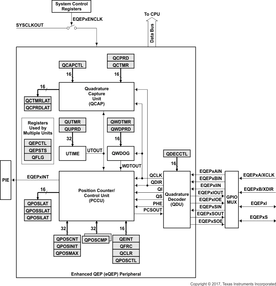
GUID-FC31593E-E4AA-4E59-BD89-84CC238C87E1-low.gifFigure 8-53 eQEP Functional Block Diagram