ZHCS009J November 2010 – September 2021 TMS320F28062 , TMS320F28062F , TMS320F28063 , TMS320F28064 , TMS320F28065 , TMS320F28066 , TMS320F28067 , TMS320F28068F , TMS320F28068M , TMS320F28069 , TMS320F28069F , TMS320F28069M
PRODUCTION DATA
- 1 特性
- 2 应用
- 3 说明
- 4 Revision History
- 5 Device Comparison
- 6 Terminal Configuration and Functions
-
7 Specifications
- 7.1 Absolute Maximum Ratings
- 7.2 ESD Ratings – Commercial
- 7.3 ESD Ratings – Automotive
- 7.4 Recommended Operating Conditions
- 7.5 Power Consumption Summary
- 7.6 Electrical Characteristics
- 7.7 Thermal Resistance Characteristics
- 7.8 Thermal Design Considerations
- 7.9 Debug Probe Connection Without Signal Buffering for the MCU
- 7.10 Parameter Information
- 7.11 Test Load Circuit
- 7.12 Power Sequencing
- 7.13 Clock Specifications
- 7.14 Flash Timing
-
8 Detailed Description
- 8.1
Overview
- 8.1.1 CPU
- 8.1.2 Control Law Accelerator (CLA)
- 8.1.3 Viterbi, Complex Math, CRC Unit (VCU)
- 8.1.4 Memory Bus (Harvard Bus Architecture)
- 8.1.5 Peripheral Bus
- 8.1.6 Real-Time JTAG and Analysis
- 8.1.7 Flash
- 8.1.8 M0, M1 SARAMs
- 8.1.9 L4 SARAM, and L0, L1, L2, L3, L5, L6, L7, and L8 DPSARAMs
- 8.1.10 Boot ROM
- 8.1.11 Security
- 8.1.12 Peripheral Interrupt Expansion (PIE) Block
- 8.1.13 External Interrupts (XINT1 to XINT3)
- 8.1.14 Internal Zero Pin Oscillators, Oscillator, and PLL
- 8.1.15 Watchdog
- 8.1.16 Peripheral Clocking
- 8.1.17 Low-power Modes
- 8.1.18 Peripheral Frames 0, 1, 2, 3 (PFn)
- 8.1.19 General-Purpose Input/Output (GPIO) Multiplexer
- 8.1.20 32-Bit CPU-Timers (0, 1, 2)
- 8.1.21 Control Peripherals
- 8.1.22 Serial Port Peripherals
- 8.2 Memory Maps
- 8.3 Register Maps
- 8.4 Device Debug Registers
- 8.5 VREG, BOR, POR
- 8.6 System Control
- 8.7 Low-power Modes Block
- 8.8 Interrupts
- 8.9
Peripherals
- 8.9.1 CLA Overview
- 8.9.2 Analog Block
- 8.9.3 Detailed Descriptions
- 8.9.4 Serial Peripheral Interface (SPI) Module
- 8.9.5 Serial Communications Interface (SCI) Module
- 8.9.6
Multichannel Buffered Serial Port (McBSP) Module
- 8.9.6.1
McBSP Electrical Data/Timing
- 8.9.6.1.1 McBSP Transmit and Receive Timing
- 8.9.6.1.2
McBSP as SPI Master or Slave Timing
- 8.9.6.1.2.1 McBSP as SPI Master or Slave Timing Requirements (CLKSTP = 10b, CLKXP = 0)
- 8.9.6.1.2.2 McBSP as SPI Master or Slave Switching Characteristics (CLKSTP = 10b, CLKXP = 0)
- 8.9.6.1.2.3 McBSP as SPI Master or Slave Timing Requirements (CLKSTP = 11b, CLKXP = 0)
- 8.9.6.1.2.4 McBSP as SPI Master or Slave Switching Characteristics (CLKSTP = 11b, CLKXP = 0)
- 8.9.6.1.2.5 McBSP as SPI Master or Slave Timing Requirements (CLKSTP = 10b, CLKXP = 1)
- 8.9.6.1.2.6 McBSP as SPI Master or Slave Switching Characteristics (CLKSTP = 10b, CLKXP = 1)
- 8.9.6.1.2.7 McBSP as SPI Master or Slave Timing Requirements (CLKSTP = 11b, CLKXP = 1)
- 8.9.6.1.2.8 McBSP as SPI Master or Slave Switching Characteristics (CLKSTP = 11b, CLKXP = 1)
- 8.9.6.1
McBSP Electrical Data/Timing
- 8.9.7 Enhanced Controller Area Network (eCAN) Module
- 8.9.8 Inter-Integrated Circuit (I2C)
- 8.9.9 Enhanced Pulse Width Modulator (ePWM) Modules (ePWM1 to ePWM8)
- 8.9.10 High-Resolution PWM (HRPWM)
- 8.9.11 Enhanced Capture Module (eCAP1)
- 8.9.12 High-Resolution Capture Modules (HRCAP1 to HRCAP4)
- 8.9.13 Enhanced Quadrature Encoder Modules (eQEP1, eQEP2)
- 8.9.14 JTAG Port
- 8.9.15 General-Purpose Input/Output (GPIO) MUX
- 8.9.16 Universal Serial Bus (USB)
- 8.1
Overview
- 9 Applications, Implementation, and Layout
- 10Device and Documentation Support
- 11Mechanical, Packaging, and Orderable Information
封装选项
机械数据 (封装 | 引脚)
散热焊盘机械数据 (封装 | 引脚)
订购信息
8.6.2 Crystal Oscillator Option
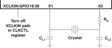
The on-chip crystal oscillator X1 and X2 pins are 1.8-V level signals and must never have 3.3-V level signals applied to them. If a system 3.3-V external oscillator is to be used as a clock source, it should be connected to the XCLKIN pin only. The X1 pin is not intended to be used as a single-ended clock input, it should be used with X2 and a crystal.
The typical specifications for the external quartz crystal (fundamental mode, parallel resonant) are listed in Table 8-12. Furthermore, ESR range = 30 to 150 Ω. For Table 8-12, Cshunt should be less than or equal to 5 pF.
| FREQUENCY (MHz) | Rd (Ω) | CL1 (pF) | CL2 (pF) |
|---|---|---|---|
| 5 | 2200 | 18 | 18 |
| 10 | 470 | 15 | 15 |
| 15 | 0 | 15 | 15 |
| 20 | 0 | 12 | 12 |
 Figure 8-12 Using the On-chip Crystal Oscillator
- CL1 and CL2 are the total capacitance of the circuit board and components excluding the IC and crystal. The value is usually approximately twice the value of the load capacitance of the crystal.
- The load capacitance of the crystal is described in the crystal specifications of the manufacturers.
- TI recommends that customers have the resonator/crystal vendor characterize the operation of their device with the MCU chip. The resonator/crystal vendor has the equipment and expertise to tune the tank circuit. The vendor can also advise the customer regarding the proper tank component values that will produce proper start-up and stability over the entire operating range.
 Figure 8-13 Using a 3.3-V External Oscillator