ZHCS009J November 2010 – September 2021 TMS320F28062 , TMS320F28062F , TMS320F28063 , TMS320F28064 , TMS320F28065 , TMS320F28066 , TMS320F28067 , TMS320F28068F , TMS320F28068M , TMS320F28069 , TMS320F28069F , TMS320F28069M
PRODUCTION DATA
- 1 特性
- 2 应用
- 3 说明
- 4 Revision History
- 5 Device Comparison
- 6 Terminal Configuration and Functions
-
7 Specifications
- 7.1 Absolute Maximum Ratings
- 7.2 ESD Ratings – Commercial
- 7.3 ESD Ratings – Automotive
- 7.4 Recommended Operating Conditions
- 7.5 Power Consumption Summary
- 7.6 Electrical Characteristics
- 7.7 Thermal Resistance Characteristics
- 7.8 Thermal Design Considerations
- 7.9 Debug Probe Connection Without Signal Buffering for the MCU
- 7.10 Parameter Information
- 7.11 Test Load Circuit
- 7.12 Power Sequencing
- 7.13 Clock Specifications
- 7.14 Flash Timing
-
8 Detailed Description
- 8.1
Overview
- 8.1.1 CPU
- 8.1.2 Control Law Accelerator (CLA)
- 8.1.3 Viterbi, Complex Math, CRC Unit (VCU)
- 8.1.4 Memory Bus (Harvard Bus Architecture)
- 8.1.5 Peripheral Bus
- 8.1.6 Real-Time JTAG and Analysis
- 8.1.7 Flash
- 8.1.8 M0, M1 SARAMs
- 8.1.9 L4 SARAM, and L0, L1, L2, L3, L5, L6, L7, and L8 DPSARAMs
- 8.1.10 Boot ROM
- 8.1.11 Security
- 8.1.12 Peripheral Interrupt Expansion (PIE) Block
- 8.1.13 External Interrupts (XINT1 to XINT3)
- 8.1.14 Internal Zero Pin Oscillators, Oscillator, and PLL
- 8.1.15 Watchdog
- 8.1.16 Peripheral Clocking
- 8.1.17 Low-power Modes
- 8.1.18 Peripheral Frames 0, 1, 2, 3 (PFn)
- 8.1.19 General-Purpose Input/Output (GPIO) Multiplexer
- 8.1.20 32-Bit CPU-Timers (0, 1, 2)
- 8.1.21 Control Peripherals
- 8.1.22 Serial Port Peripherals
- 8.2 Memory Maps
- 8.3 Register Maps
- 8.4 Device Debug Registers
- 8.5 VREG, BOR, POR
- 8.6 System Control
- 8.7 Low-power Modes Block
- 8.8 Interrupts
- 8.9
Peripherals
- 8.9.1 CLA Overview
- 8.9.2 Analog Block
- 8.9.3 Detailed Descriptions
- 8.9.4 Serial Peripheral Interface (SPI) Module
- 8.9.5 Serial Communications Interface (SCI) Module
- 8.9.6
Multichannel Buffered Serial Port (McBSP) Module
- 8.9.6.1
McBSP Electrical Data/Timing
- 8.9.6.1.1 McBSP Transmit and Receive Timing
- 8.9.6.1.2
McBSP as SPI Master or Slave Timing
- 8.9.6.1.2.1 McBSP as SPI Master or Slave Timing Requirements (CLKSTP = 10b, CLKXP = 0)
- 8.9.6.1.2.2 McBSP as SPI Master or Slave Switching Characteristics (CLKSTP = 10b, CLKXP = 0)
- 8.9.6.1.2.3 McBSP as SPI Master or Slave Timing Requirements (CLKSTP = 11b, CLKXP = 0)
- 8.9.6.1.2.4 McBSP as SPI Master or Slave Switching Characteristics (CLKSTP = 11b, CLKXP = 0)
- 8.9.6.1.2.5 McBSP as SPI Master or Slave Timing Requirements (CLKSTP = 10b, CLKXP = 1)
- 8.9.6.1.2.6 McBSP as SPI Master or Slave Switching Characteristics (CLKSTP = 10b, CLKXP = 1)
- 8.9.6.1.2.7 McBSP as SPI Master or Slave Timing Requirements (CLKSTP = 11b, CLKXP = 1)
- 8.9.6.1.2.8 McBSP as SPI Master or Slave Switching Characteristics (CLKSTP = 11b, CLKXP = 1)
- 8.9.6.1
McBSP Electrical Data/Timing
- 8.9.7 Enhanced Controller Area Network (eCAN) Module
- 8.9.8 Inter-Integrated Circuit (I2C)
- 8.9.9 Enhanced Pulse Width Modulator (ePWM) Modules (ePWM1 to ePWM8)
- 8.9.10 High-Resolution PWM (HRPWM)
- 8.9.11 Enhanced Capture Module (eCAP1)
- 8.9.12 High-Resolution Capture Modules (HRCAP1 to HRCAP4)
- 8.9.13 Enhanced Quadrature Encoder Modules (eQEP1, eQEP2)
- 8.9.14 JTAG Port
- 8.9.15 General-Purpose Input/Output (GPIO) MUX
- 8.9.16 Universal Serial Bus (USB)
- 8.1
Overview
- 9 Applications, Implementation, and Layout
- 10Device and Documentation Support
- 11Mechanical, Packaging, and Orderable Information
封装选项
机械数据 (封装 | 引脚)
散热焊盘机械数据 (封装 | 引脚)
订购信息
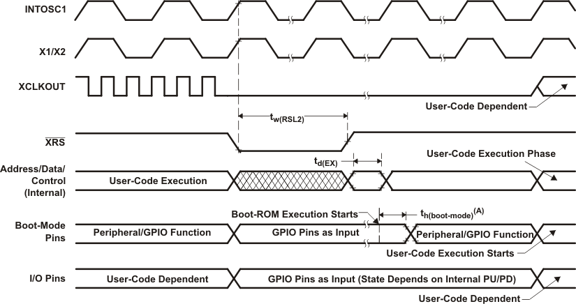
7.12.2 Reset ( XRS) Switching Characteristics
over recommended operating conditions (unless otherwise noted)
| PARAMETER | MIN | TYP | MAX | UNIT | |
|---|---|---|---|---|---|
| tw(RSL1) | Pulse duration, XRS driven by device | 600 | μs | ||
| tw(WDRS) | Pulse duration, reset pulse generated by watchdog | 512tc(OSCCLK) | cycles | ||
| td(EX) | Delay time, address/data valid after XRS high | 32tc(OSCCLK) | cycles | ||
| tINTOSCST | Start-up time, internal zero-pin oscillator | 3 | μs | ||
| tOSCST(1) | On-chip crystal-oscillator start-up time | 1 | 10 | ms | |
(1) Dependent on crystal/resonator and board design.

After reset, the Boot ROM code samples BOOT Mode pins. Based on the status of the Boot Mode pin, the boot code branches to destination memory or boot code function. If Boot ROM code executes after power-on conditions (in debugger environment), the Boot code execution time is based on the current SYSCLKOUT speed. The SYSCLKOUT will be based on user environment and could be with or without PLL enabled.
Figure 7-6 Warm ResetFigure 7-7 shows an example for the effect of writing into PLLCR register. In the first phase, PLLCR = 0x0004 and SYSCLKOUT = OSCCLK × 2. The PLLCR is then written with 0x0008. Right after the PLLCR register is written, the PLL lock-up phase begins. During this phase, SYSCLKOUT = OSCCLK/2. After the PLL lock-up is complete, SYSCLKOUT reflects the new operating frequency, OSCCLK × 4.
 Figure 7-7 Example of Effect of Writing Into PLLCR Register