ZHCS898O October 2003 – March 2019 TMS320F2801 , TMS320F28015 , TMS320F28016 , TMS320F2802 , TMS320F2806 , TMS320F2808 , TMS320F2809
PRODUCTION DATA.
- 1器件概述
- 2修订历史记录
- 3Device Comparison
- 4Terminal Configuration and Functions
-
5Specifications
- 5.1 Absolute Maximum Ratings
- 5.2 ESD Ratings – Automotive
- 5.3 ESD Ratings – Commercial
- 5.4 Recommended Operating Conditions
- 5.5
Power Consumption Summary
- Table 5-1 TMS320F2809, TMS320F2808 Current Consumption by Power-Supply Pins at 100-MHz SYSCLKOUT
- Table 5-2 TMS320F2806 Current Consumption by Power-Supply Pins at 100-MHz SYSCLKOUT
- Table 5-3 TMS320F2802, TMS320F2801 Current Consumption by Power-Supply Pins at 100-MHz SYSCLKOUT
- Table 5-4 TMS320C2802, TMS320C2801 Current Consumption by Power-Supply Pins at 100-MHz SYSCLKOUT
- 5.5.1 Reducing Current Consumption
- 5.5.2 Current Consumption Graphs
- 5.6 Electrical Characteristics
- 5.7 Thermal Resistance Characteristics for F280x 100-Ball GGM Package
- 5.8 Thermal Resistance Characteristics for F280x 100-Pin PZ Package
- 5.9 Thermal Resistance Characteristics for C280x 100-Ball GGM Package
- 5.10 Thermal Resistance Characteristics for C280x 100-Pin PZ Package
- 5.11 Thermal Resistance Characteristics for F2809 100-Ball GGM Package
- 5.12 Thermal Resistance Characteristics for F2809 100-Pin PZ Package
- 5.13 Thermal Design Considerations
- 5.14
Timing and Switching Characteristics
- 5.14.1 Timing Parameter Symbology
- 5.14.2 Power Sequencing
- 5.14.3 Clock Requirements and Characteristics
- 5.14.4
Peripherals
- 5.14.4.1 General-Purpose Input/Output (GPIO)
- 5.14.4.2 Enhanced Control Peripherals
- 5.14.4.3 External Interrupt Timing
- 5.14.4.4 I2C Electrical Specification and Timing
- 5.14.4.5 Serial Peripheral Interface (SPI) Timing
- 5.14.5 Emulator Connection Without Signal Buffering for the DSP
- 5.14.6 Flash Timing
- 5.15 On-Chip Analog-to-Digital Converter
- 5.16 Migrating From F280x Devices to C280x Devices
- 5.17 ROM Timing (C280x only)
-
6Detailed Description
- 6.1
Brief Descriptions
- 6.1.1 C28x CPU
- 6.1.2 Memory Bus (Harvard Bus Architecture)
- 6.1.3 Peripheral Bus
- 6.1.4 Real-Time JTAG and Analysis
- 6.1.5 Flash
- 6.1.6 ROM
- 6.1.7 M0, M1 SARAMs
- 6.1.8 L0, L1, H0 SARAMs
- 6.1.9 Boot ROM
- 6.1.10 Security
- 6.1.11 Peripheral Interrupt Expansion (PIE) Block
- 6.1.12 External Interrupts (XINT1, XINT2, XNMI)
- 6.1.13 Oscillator and PLL
- 6.1.14 Watchdog
- 6.1.15 Peripheral Clocking
- 6.1.16 Low-Power Modes
- 6.1.17 Peripheral Frames 0, 1, 2 (PFn)
- 6.1.18 General-Purpose Input/Output (GPIO) Multiplexer
- 6.1.19 32-Bit CPU-Timers (0, 1, 2)
- 6.1.20 Control Peripherals
- 6.1.21 Serial Port Peripherals
- 6.2
Peripherals
- 6.2.1 32-Bit CPU-Timers 0/1/2
- 6.2.2 Enhanced PWM Modules (ePWM1/2/3/4/5/6)
- 6.2.3 Hi-Resolution PWM (HRPWM)
- 6.2.4 Enhanced CAP Modules (eCAP1/2/3/4)
- 6.2.5 Enhanced QEP Modules (eQEP1/2)
- 6.2.6 Enhanced Analog-to-Digital Converter (ADC) Module
- 6.2.7 Enhanced Controller Area Network (eCAN) Modules (eCAN-A and eCAN-B)
- 6.2.8 Serial Communications Interface (SCI) Modules (SCI-A, SCI-B)
- 6.2.9 Serial Peripheral Interface (SPI) Modules (SPI-A, SPI-B, SPI-C, SPI-D)
- 6.2.10 Inter-Integrated Circuit (I2C)
- 6.2.11 GPIO MUX
- 6.3 Memory Maps
- 6.4 Register Map
- 6.5 Interrupts
- 6.6 System Control
- 6.7 Low-Power Modes Block
- 6.1
Brief Descriptions
- 7Applications, Implementation, and Layout
- 8器件和文档支持
- 9机械、封装和可订购信息
封装选项
请参考 PDF 数据表获取器件具体的封装图。
机械数据 (封装 | 引脚)
- PZ|100
散热焊盘机械数据 (封装 | 引脚)
- PZ|100
订购信息
6.2.2 Enhanced PWM Modules (ePWM1/2/3/4/5/6)
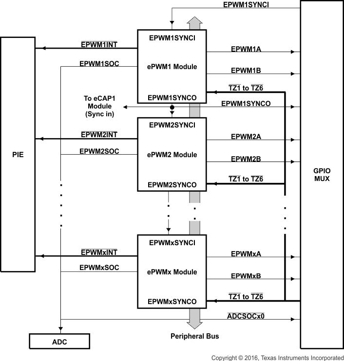
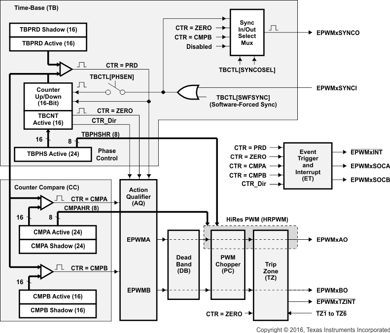
The 280x device contains up to six enhanced PWM modules (ePWM). Figure 6-3 shows a block diagram of multiple ePWM modules. Figure 6-4 shows the signal interconnections with the ePWM. See the TMS320x280x, 2801x, 2804x Enhanced Pulse Width Modulator (ePWM) module reference guide for more details.
 Figure 6-3 Multiple PWM Modules in a 280x System
 Table 6-3 shows the complete ePWM register set per module.
Table 6-3 ePWM Control and Status Registers
| NAME | ePWM1 | ePWM2 | ePWM3 | ePWM4 | ePWM5 | ePWM6 | SIZE (x16) / #SHADOW | DESCRIPTION |
|---|---|---|---|---|---|---|---|---|
| TBCTL | 0x6800 | 0x6840 | 0x6880 | 0x68C0 | 0x6900 | 0x6940 | 1 / 0 | Time Base Control Register |
| TBSTS | 0x6801 | 0x6841 | 0x6881 | 0x68C1 | 0x6901 | 0x6941 | 1 / 0 | Time Base Status Register |
| TBPHSHR | 0x6802 | 0x6842 | 0x6882 | 0x68C2 | N/A | N/A | 1 / 0 | Time Base Phase HRPWM Register |
| TBPHS | 0x6803 | 0x6843 | 0x6883 | 0x68C3 | 0x6903 | 0x6943 | 1 / 0 | Time Base Phase Register |
| TBCTR | 0x6804 | 0x6844 | 0x6884 | 0x68C4 | 0x6904 | 0x6944 | 1 / 0 | Time Base Counter Register |
| TBPRD | 0x6805 | 0x6845 | 0x6885 | 0x68C5 | 0x6905 | 0x6945 | 1 / 1 | Time Base Period Register Set |
| CMPCTL | 0x6807 | 0x6847 | 0x6887 | 0x68C7 | 0x6907 | 0x6947 | 1 / 0 | Counter Compare Control Register |
| CMPAHR | 0x6808 | 0x6848 | 0x6888 | 0x68C8 | N/A | N/A | 1 / 1 | Time Base Compare A HRPWM Register |
| CMPA | 0x6809 | 0x6849 | 0x6889 | 0x68C9 | 0x6909 | 0x6949 | 1 / 1 | Counter Compare A Register Set |
| CMPB | 0x680A | 0x684A | 0x688A | 0x68CA | 0x690A | 0x694A | 1 / 1 | Counter Compare B Register Set |
| AQCTLA | 0x680B | 0x684B | 0x688B | 0x68CB | 0x690B | 0x694B | 1 / 0 | Action Qualifier Control Register For Output A |
| AQCTLB | 0x680C | 0x684C | 0x688C | 0x68CC | 0x690C | 0x694C | 1 / 0 | Action Qualifier Control Register For Output B |
| AQSFRC | 0x680D | 0x684D | 0x688D | 0x68CD | 0x690D | 0x694D | 1 / 0 | Action Qualifier Software Force Register |
| AQCSFRC | 0x680E | 0x684E | 0x688E | 0x68CE | 0x690E | 0x694E | 1 / 1 | Action Qualifier Continuous S/W Force Register Set |
| DBCTL | 0x680F | 0x684F | 0x688F | 0x68CF | 0x690F | 0x694F | 1 / 1 | Dead-Band Generator Control Register |
| DBRED | 0x6810 | 0x6850 | 0x6890 | 0x68D0 | 0x6910 | 0x6950 | 1 / 0 | Dead-Band Generator Rising Edge Delay Count Register |
| DBFED | 0x6811 | 0x6851 | 0x6891 | 0x68D1 | 0x6911 | 0x6951 | 1 / 0 | Dead-Band Generator Falling Edge Delay Count Register |
| TZSEL | 0x6812 | 0x6852 | 0x6892 | 0x68D2 | 0x6912 | 0x6952 | 1 / 0 | Trip Zone Select Register(1) |
| TZCTL | 0x6814 | 0x6854 | 0x6894 | 0x68D4 | 0x6914 | 0x6954 | 1 / 0 | Trip Zone Control Register(1) |
| TZEINT | 0x6815 | 0x6855 | 0x6895 | 0x68D5 | 0x6915 | 0x6955 | 1 / 0 | Trip Zone Enable Interrupt Register(1) |
| TZFLG | 0x6816 | 0x6856 | 0x6896 | 0x68D6 | 0x6916 | 0x6956 | 1 / 0 | Trip Zone Flag Register |
| TZCLR | 0x6817 | 0x6857 | 0x6897 | 0x68D7 | 0x6917 | 0x6957 | 1 / 0 | Trip Zone Clear Register(1) |
| TZFRC | 0x6818 | 0x6858 | 0x6898 | 0x68D8 | 0x6918 | 0x6958 | 1 / 0 | Trip Zone Force Register(1) |
| ETSEL | 0x6819 | 0x6859 | 0x6899 | 0x68D9 | 0x6919 | 0x6959 | 1 / 0 | Event Trigger Selection Register |
| ETPS | 0x681A | 0x685A | 0x689A | 0x68DA | 0x691A | 0x695A | 1 / 0 | Event Trigger Prescale Register |
| ETFLG | 0x681B | 0x685B | 0x689B | 0x68DB | 0x691B | 0x695B | 1 / 0 | Event Trigger Flag Register |
| ETCLR | 0x681C | 0x685C | 0x689C | 0x68DC | 0x691C | 0x695C | 1 / 0 | Event Trigger Clear Register |
| ETFRC | 0x681D | 0x685D | 0x689D | 0x68DD | 0x691D | 0x695D | 1 / 0 | Event Trigger Force Register |
| PCCTL | 0x681E | 0x685E | 0x689E | 0x68DE | 0x691E | 0x695E | 1 / 0 | PWM Chopper Control Register |
| HRCNFG | 0x6820 | 0x6860 | 0x68A0 | 0x68E0 | 0x6920(2) | 0x6960(2) | 1 / 0 | HRPWM Configuration Register(1) |
(1) Registers that are EALLOW protected.
(2) Applicable to F2809 only
 Figure 6-4 ePWM Sub-Modules Showing Critical Internal Signal Interconnections