ZHCS898O October 2003 – March 2019 TMS320F2801 , TMS320F28015 , TMS320F28016 , TMS320F2802 , TMS320F2806 , TMS320F2808 , TMS320F2809
PRODUCTION DATA.
- 1器件概述
- 2修订历史记录
- 3Device Comparison
- 4Terminal Configuration and Functions
-
5Specifications
- 5.1 Absolute Maximum Ratings
- 5.2 ESD Ratings – Automotive
- 5.3 ESD Ratings – Commercial
- 5.4 Recommended Operating Conditions
- 5.5
Power Consumption Summary
- Table 5-1 TMS320F2809, TMS320F2808 Current Consumption by Power-Supply Pins at 100-MHz SYSCLKOUT
- Table 5-2 TMS320F2806 Current Consumption by Power-Supply Pins at 100-MHz SYSCLKOUT
- Table 5-3 TMS320F2802, TMS320F2801 Current Consumption by Power-Supply Pins at 100-MHz SYSCLKOUT
- Table 5-4 TMS320C2802, TMS320C2801 Current Consumption by Power-Supply Pins at 100-MHz SYSCLKOUT
- 5.5.1 Reducing Current Consumption
- 5.5.2 Current Consumption Graphs
- 5.6 Electrical Characteristics
- 5.7 Thermal Resistance Characteristics for F280x 100-Ball GGM Package
- 5.8 Thermal Resistance Characteristics for F280x 100-Pin PZ Package
- 5.9 Thermal Resistance Characteristics for C280x 100-Ball GGM Package
- 5.10 Thermal Resistance Characteristics for C280x 100-Pin PZ Package
- 5.11 Thermal Resistance Characteristics for F2809 100-Ball GGM Package
- 5.12 Thermal Resistance Characteristics for F2809 100-Pin PZ Package
- 5.13 Thermal Design Considerations
- 5.14
Timing and Switching Characteristics
- 5.14.1 Timing Parameter Symbology
- 5.14.2 Power Sequencing
- 5.14.3 Clock Requirements and Characteristics
- 5.14.4
Peripherals
- 5.14.4.1 General-Purpose Input/Output (GPIO)
- 5.14.4.2 Enhanced Control Peripherals
- 5.14.4.3 External Interrupt Timing
- 5.14.4.4 I2C Electrical Specification and Timing
- 5.14.4.5 Serial Peripheral Interface (SPI) Timing
- 5.14.5 Emulator Connection Without Signal Buffering for the DSP
- 5.14.6 Flash Timing
- 5.15 On-Chip Analog-to-Digital Converter
- 5.16 Migrating From F280x Devices to C280x Devices
- 5.17 ROM Timing (C280x only)
-
6Detailed Description
- 6.1
Brief Descriptions
- 6.1.1 C28x CPU
- 6.1.2 Memory Bus (Harvard Bus Architecture)
- 6.1.3 Peripheral Bus
- 6.1.4 Real-Time JTAG and Analysis
- 6.1.5 Flash
- 6.1.6 ROM
- 6.1.7 M0, M1 SARAMs
- 6.1.8 L0, L1, H0 SARAMs
- 6.1.9 Boot ROM
- 6.1.10 Security
- 6.1.11 Peripheral Interrupt Expansion (PIE) Block
- 6.1.12 External Interrupts (XINT1, XINT2, XNMI)
- 6.1.13 Oscillator and PLL
- 6.1.14 Watchdog
- 6.1.15 Peripheral Clocking
- 6.1.16 Low-Power Modes
- 6.1.17 Peripheral Frames 0, 1, 2 (PFn)
- 6.1.18 General-Purpose Input/Output (GPIO) Multiplexer
- 6.1.19 32-Bit CPU-Timers (0, 1, 2)
- 6.1.20 Control Peripherals
- 6.1.21 Serial Port Peripherals
- 6.2
Peripherals
- 6.2.1 32-Bit CPU-Timers 0/1/2
- 6.2.2 Enhanced PWM Modules (ePWM1/2/3/4/5/6)
- 6.2.3 Hi-Resolution PWM (HRPWM)
- 6.2.4 Enhanced CAP Modules (eCAP1/2/3/4)
- 6.2.5 Enhanced QEP Modules (eQEP1/2)
- 6.2.6 Enhanced Analog-to-Digital Converter (ADC) Module
- 6.2.7 Enhanced Controller Area Network (eCAN) Modules (eCAN-A and eCAN-B)
- 6.2.8 Serial Communications Interface (SCI) Modules (SCI-A, SCI-B)
- 6.2.9 Serial Peripheral Interface (SPI) Modules (SPI-A, SPI-B, SPI-C, SPI-D)
- 6.2.10 Inter-Integrated Circuit (I2C)
- 6.2.11 GPIO MUX
- 6.3 Memory Maps
- 6.4 Register Map
- 6.5 Interrupts
- 6.6 System Control
- 6.7 Low-Power Modes Block
- 6.1
Brief Descriptions
- 7Applications, Implementation, and Layout
- 8器件和文档支持
- 9机械、封装和可订购信息
封装选项
请参考 PDF 数据表获取器件具体的封装图。
机械数据 (封装 | 引脚)
- PZ|100
- GBA|100
- NMF|100
散热焊盘机械数据 (封装 | 引脚)
- PZ|100
订购信息
6.2.5 Enhanced QEP Modules (eQEP1/2)
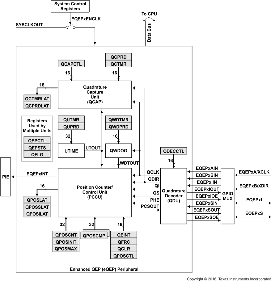
The 280x device contains up to two enhanced quadrature encoder (eQEP) modules. See the TMS320x280x, 2801x, 2804x Enhanced Quadrature Encoder Pulse (eQEP) module reference guide for more details.
 Figure 6-6 eQEP Functional Block Diagram
 Table 6-5 provides a summary of the eQEP registers.
Table 6-5 eQEP Control and Status Registers
| NAME | eQEP1
ADDRESS |
eQEP2
ADDRESS |
eQEP1
SIZE(x16)/ #SHADOW |
REGISTER DESCRIPTION |
|---|---|---|---|---|
| QPOSCNT | 0x6B00 | 0x6B40 | 2/0 | eQEP Position Counter |
| QPOSINIT | 0x6B02 | 0x6B42 | 2/0 | eQEP Initialization Position Count |
| QPOSMAX | 0x6B04 | 0x6B44 | 2/0 | eQEP Maximum Position Count |
| QPOSCMP | 0x6B06 | 0x6B46 | 2/1 | eQEP Position-compare |
| QPOSILAT | 0x6B08 | 0x6B48 | 2/0 | eQEP Index Position Latch |
| QPOSSLAT | 0x6B0A | 0x6B4A | 2/0 | eQEP Strobe Position Latch |
| QPOSLAT | 0x6B0C | 0x6B4C | 2/0 | eQEP Position Latch |
| QUTMR | 0x6B0E | 0x6B4E | 2/0 | eQEP Unit Timer |
| QUPRD | 0x6B10 | 0x6B50 | 2/0 | eQEP Unit Period Register |
| QWDTMR | 0x6B12 | 0x6B52 | 1/0 | eQEP Watchdog Timer |
| QWDPRD | 0x6B13 | 0x6B53 | 1/0 | eQEP Watchdog Period Register |
| QDECCTL | 0x6B14 | 0x6B54 | 1/0 | eQEP Decoder Control Register |
| QEPCTL | 0x6B15 | 0x6B55 | 1/0 | eQEP Control Register |
| QCAPCTL | 0x6B16 | 0x6B56 | 1/0 | eQEP Capture Control Register |
| QPOSCTL | 0x6B17 | 0x6B57 | 1/0 | eQEP Position-compare Control Register |
| QEINT | 0x6B18 | 0x6B58 | 1/0 | eQEP Interrupt Enable Register |
| QFLG | 0x6B19 | 0x6B59 | 1/0 | eQEP Interrupt Flag Register |
| QCLR | 0x6B1A | 0x6B5A | 1/0 | eQEP Interrupt Clear Register |
| QFRC | 0x6B1B | 0x6B5B | 1/0 | eQEP Interrupt Force Register |
| QEPSTS | 0x6B1C | 0x6B5C | 1/0 | eQEP Status Register |
| QCTMR | 0x6B1D | 0x6B5D | 1/0 | eQEP Capture Timer |
| QCPRD | 0x6B1E | 0x6B5E | 1/0 | eQEP Capture Period Register |
| QCTMRLAT | 0x6B1F | 0x6B5F | 1/0 | eQEP Capture Timer Latch |
| QCPRDLAT | 0x6B20 | 0x6B60 | 1/0 | eQEP Capture Period Latch |
| Reserved | 0x6B21– 0x6B3F | 0x6B61 – 0x6B7F | 31/0 | Reserved |