ZHCS898O October 2003 – March 2019 TMS320F2801 , TMS320F28015 , TMS320F28016 , TMS320F2802 , TMS320F2806 , TMS320F2808 , TMS320F2809
PRODUCTION DATA.
- 1器件概述
- 2修订历史记录
- 3Device Comparison
- 4Terminal Configuration and Functions
-
5Specifications
- 5.1 Absolute Maximum Ratings
- 5.2 ESD Ratings – Automotive
- 5.3 ESD Ratings – Commercial
- 5.4 Recommended Operating Conditions
- 5.5
Power Consumption Summary
- Table 5-1 TMS320F2809, TMS320F2808 Current Consumption by Power-Supply Pins at 100-MHz SYSCLKOUT
- Table 5-2 TMS320F2806 Current Consumption by Power-Supply Pins at 100-MHz SYSCLKOUT
- Table 5-3 TMS320F2802, TMS320F2801 Current Consumption by Power-Supply Pins at 100-MHz SYSCLKOUT
- Table 5-4 TMS320C2802, TMS320C2801 Current Consumption by Power-Supply Pins at 100-MHz SYSCLKOUT
- 5.5.1 Reducing Current Consumption
- 5.5.2 Current Consumption Graphs
- 5.6 Electrical Characteristics
- 5.7 Thermal Resistance Characteristics for F280x 100-Ball GGM Package
- 5.8 Thermal Resistance Characteristics for F280x 100-Pin PZ Package
- 5.9 Thermal Resistance Characteristics for C280x 100-Ball GGM Package
- 5.10 Thermal Resistance Characteristics for C280x 100-Pin PZ Package
- 5.11 Thermal Resistance Characteristics for F2809 100-Ball GGM Package
- 5.12 Thermal Resistance Characteristics for F2809 100-Pin PZ Package
- 5.13 Thermal Design Considerations
- 5.14
Timing and Switching Characteristics
- 5.14.1 Timing Parameter Symbology
- 5.14.2 Power Sequencing
- 5.14.3 Clock Requirements and Characteristics
- 5.14.4
Peripherals
- 5.14.4.1 General-Purpose Input/Output (GPIO)
- 5.14.4.2 Enhanced Control Peripherals
- 5.14.4.3 External Interrupt Timing
- 5.14.4.4 I2C Electrical Specification and Timing
- 5.14.4.5 Serial Peripheral Interface (SPI) Timing
- 5.14.5 Emulator Connection Without Signal Buffering for the DSP
- 5.14.6 Flash Timing
- 5.15 On-Chip Analog-to-Digital Converter
- 5.16 Migrating From F280x Devices to C280x Devices
- 5.17 ROM Timing (C280x only)
-
6Detailed Description
- 6.1
Brief Descriptions
- 6.1.1 C28x CPU
- 6.1.2 Memory Bus (Harvard Bus Architecture)
- 6.1.3 Peripheral Bus
- 6.1.4 Real-Time JTAG and Analysis
- 6.1.5 Flash
- 6.1.6 ROM
- 6.1.7 M0, M1 SARAMs
- 6.1.8 L0, L1, H0 SARAMs
- 6.1.9 Boot ROM
- 6.1.10 Security
- 6.1.11 Peripheral Interrupt Expansion (PIE) Block
- 6.1.12 External Interrupts (XINT1, XINT2, XNMI)
- 6.1.13 Oscillator and PLL
- 6.1.14 Watchdog
- 6.1.15 Peripheral Clocking
- 6.1.16 Low-Power Modes
- 6.1.17 Peripheral Frames 0, 1, 2 (PFn)
- 6.1.18 General-Purpose Input/Output (GPIO) Multiplexer
- 6.1.19 32-Bit CPU-Timers (0, 1, 2)
- 6.1.20 Control Peripherals
- 6.1.21 Serial Port Peripherals
- 6.2
Peripherals
- 6.2.1 32-Bit CPU-Timers 0/1/2
- 6.2.2 Enhanced PWM Modules (ePWM1/2/3/4/5/6)
- 6.2.3 Hi-Resolution PWM (HRPWM)
- 6.2.4 Enhanced CAP Modules (eCAP1/2/3/4)
- 6.2.5 Enhanced QEP Modules (eQEP1/2)
- 6.2.6 Enhanced Analog-to-Digital Converter (ADC) Module
- 6.2.7 Enhanced Controller Area Network (eCAN) Modules (eCAN-A and eCAN-B)
- 6.2.8 Serial Communications Interface (SCI) Modules (SCI-A, SCI-B)
- 6.2.9 Serial Peripheral Interface (SPI) Modules (SPI-A, SPI-B, SPI-C, SPI-D)
- 6.2.10 Inter-Integrated Circuit (I2C)
- 6.2.11 GPIO MUX
- 6.3 Memory Maps
- 6.4 Register Map
- 6.5 Interrupts
- 6.6 System Control
- 6.7 Low-Power Modes Block
- 6.1
Brief Descriptions
- 7Applications, Implementation, and Layout
- 8器件和文档支持
- 9机械、封装和可订购信息
封装选项
请参考 PDF 数据表获取器件具体的封装图。
机械数据 (封装 | 引脚)
- PZ|100
- NMF|100
散热焊盘机械数据 (封装 | 引脚)
- PZ|100
订购信息
6.2.10 Inter-Integrated Circuit (I2C)
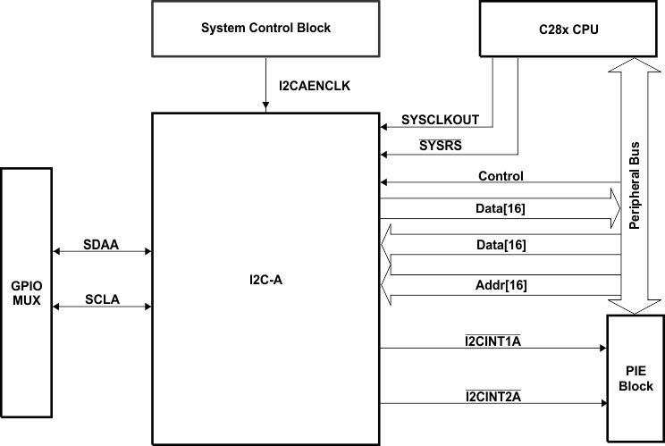
The 280x device contains one I2C Serial Port. Figure 6-15 shows how the I2C peripheral module interfaces within the 280x device.
The I2C module has the following features:
- Compliance with the Philips Semiconductors I2C-bus specification (version 2.1):
- Support for 1-bit to 8-bit format transfers
- 7-bit and 10-bit addressing modes
- General call
- START byte mode
- Support for multiple master-transmitters and slave-receivers
- Support for multiple slave-transmitters and master-receivers
- Combined master transmit/receive and receive/transmit mode
- Data transfer rate of from 10 kbps up to 400 kbps (I2C Fast-mode rate)
- One 16-word receive FIFO and one 16-word transmit FIFO
- One interrupt that can be used by the CPU. This interrupt can be generated as a result of one of the following conditions:
- Transmit-data ready
- Receive-data ready
- Register-access ready
- No-acknowledgment received
- Arbitration lost
- Stop condition detected
- Addressed as slave
- An additional interrupt that can be used by the CPU when in FIFO mode
- Module enable/disable capability
- Free data format mode

A. The I2C registers are accessed at the SYSCLKOUT rate. The internal timing and signal waveforms of the I2C port are also at the SYSCLKOUT rate.
B. The clock enable bit (I2CAENCLK) in the PCLKCRO register turns off the clock to the I2C port for low power operation. Upon reset, I2CAENCLK is clear, which indicates the peripheral internal clocks are off.
Figure 6-15 I2C Peripheral Module Interfaces The registers in Table 6-15 configure and control the I2C port operation.
Table 6-15 I2C-A Registers
| NAME | ADDRESS | DESCRIPTION |
|---|---|---|
| I2COAR | 0x7900 | I2C own address register |
| I2CIER | 0x7901 | I2C interrupt enable register |
| I2CSTR | 0x7902 | I2C status register |
| I2CCLKL | 0x7903 | I2C clock low-time divider register |
| I2CCLKH | 0x7904 | I2C clock high-time divider register |
| I2CCNT | 0x7905 | I2C data count register |
| I2CDRR | 0x7906 | I2C data receive register |
| I2CSAR | 0x7907 | I2C slave address register |
| I2CDXR | 0x7908 | I2C data transmit register |
| I2CMDR | 0x7909 | I2C mode register |
| I2CISRC | 0x790A | I2C interrupt source register |
| I2CPSC | 0x790C | I2C prescaler register |
| I2CFFTX | 0x7920 | I2C FIFO transmit register |
| I2CFFRX | 0x7921 | I2C FIFO receive register |
| I2CRSR | - | I2C receive shift register (not accessible to the CPU) |
| I2CXSR | - | I2C transmit shift register (not accessible to the CPU) |