ZHCS894U April 2001 – July 2019 TMS320F2810 , TMS320F2811 , TMS320F2812
PRODUCTION DATA.
- 1器件概述
- 2修订历史记录
- 3Device Comparison
- 4Terminal Configuration and Functions
-
5Specifications
- 5.1 Absolute Maximum Ratings
- 5.2 ESD Ratings – Commercial
- 5.3 ESD Ratings – Automotive
- 5.4 Recommended Operating Conditions
- 5.5 Power Consumption Summary
- 5.6 Electrical Characteristics
- 5.7 Thermal Resistance Characteristics for 179-Ball ZHH Package
- 5.8 Thermal Resistance Characteristics for 179-Ball GHH Package
- 5.9 Thermal Resistance Characteristics for 176-Pin PGF Package
- 5.10 Thermal Resistance Characteristics for 128-Pin PBK Package
- 5.11 Thermal Design Considerations
- 5.12
Timing and Switching Characteristics
- 5.12.1 Timing Parameter Symbology
- 5.12.2 Power Supply Sequencing
- 5.12.3 Reset Timing
- 5.12.4 Clock Specifications
- 5.12.5
Peripherals
- 5.12.5.1 General-Purpose Input/Output (GPIO) – Output Timing
- 5.12.5.2 General-Purpose Input/Output (GPIO) – Input Timing
- 5.12.5.3 Event Manager Interface
- 5.12.5.4 Low-Power Mode Wakeup Timing
- 5.12.5.5 Serial Peripheral Interface (SPI) Master Mode Timing
- 5.12.5.6 Serial Peripheral Interface (SPI) Slave Mode Timing
- 5.12.5.7 External Interface (XINTF) Timing
- 5.12.5.8 XINTF Signal Alignment to XCLKOUT
- 5.12.5.9 External Interface Read Timing
- 5.12.5.10 External Interface Write Timing
- 5.12.5.11
External Interface Ready-on-Read Timing With One External Wait State
- Table 5-31 External Memory Interface Read Switching Characteristics (Ready-on-Read, 1 Wait State)
- Table 5-32 External Memory Interface Read Timing Requirements (Ready-on-Read, 1 Wait State)
- Table 5-33 Synchronous XREADY Timing Requirements (Ready-on-Read, 1 Wait State)
- Table 5-34 Asynchronous XREADY Timing Requirements (Ready-on-Read, 1 Wait State)
- 5.12.5.12 External Interface Ready-on-Write Timing With One External Wait State
- 5.12.5.13 XHOLD and XHOLDA
- 5.12.5.14 XHOLD/XHOLDA Timing
- 5.12.5.15
On-Chip Analog-to-Digital Converter
- Table 5-40 ADC Absolute Maximum Ratings Over Recommended Operating Conditions (Unless Otherwise Noted)
- Table 5-41 ADC Electrical Characteristics Over Recommended Operating Conditions (Unless Otherwise Noted)—AC Specifications
- Table 5-42 ADC Electrical Characteristics Over Recommended Operating Conditions (Unless Otherwise Noted)—DC Specifications
- 5.12.5.15.1 Current Consumption for Different ADC Configurations
- 5.12.5.15.2 ADC Power-Up Control Bit Timing
- 5.12.5.15.3 Detailed Description
- 5.12.5.15.4 Sequential Sampling Mode (Single-Channel) (SMODE = 0)
- 5.12.5.15.5 Simultaneous Sampling Mode (Dual-Channel) (SMODE = 1)
- 5.12.5.15.6 Definitions of Specifications and Terminology
- 5.12.5.16
Multichannel Buffered Serial Port (McBSP) Timing
- 5.12.5.16.1 McBSP Transmit and Receive Timing
- 5.12.5.16.2
McBSP as SPI Master or Slave Timing
- Table 5-49 McBSP as SPI Master or Slave Timing Requirements (CLKSTP = 10b, CLKXP = 0)
- Table 5-50 McBSP as SPI Master or Slave Switching Characteristics (CLKSTP = 10b, CLKXP = 0)
- Table 5-51 McBSP as SPI Master or Slave Timing Requirements (CLKSTP = 11b, CLKXP = 0)
- Table 5-52 McBSP as SPI Master or Slave Switching Characteristics (CLKSTP = 11b, CLKXP = 0)
- Table 5-53 McBSP as SPI Master or Slave Timing Requirements (CLKSTP = 10b, CLKXP = 1)
- Table 5-54 McBSP as SPI Master or Slave Switching Characteristics (CLKSTP = 10b, CLKXP = 1)
- Table 5-55 McBSP as SPI Master or Slave Timing Requirements (CLKSTP = 11b, CLKXP = 1)
- Table 5-56 McBSP as SPI Master or Slave Switching Characteristics (CLKSTP = 11b, CLKXP = 1)
- 5.12.6 Emulator Connection Without Signal Buffering for the DSP
- 5.12.7 Interrupt Timing
- 5.12.8 Flash Timing
-
6Detailed Description
- 6.1
Brief Descriptions
- 6.1.1 C28x CPU
- 6.1.2 Memory Bus (Harvard Bus Architecture)
- 6.1.3 Peripheral Bus
- 6.1.4 Real-Time JTAG and Analysis
- 6.1.5 External Interface (XINTF) (F2812 Only)
- 6.1.6 Flash
- 6.1.7 M0, M1 SARAMs
- 6.1.8 L0, L1, H0 SARAMs
- 6.1.9 Boot ROM
- 6.1.10 Security
- 6.1.11 Peripheral Interrupt Expansion (PIE) Block
- 6.1.12 External Interrupts (XINT1, XINT2, XINT13, XNMI)
- 6.1.13 Oscillator and PLL
- 6.1.14 Watchdog
- 6.1.15 Peripheral Clocking
- 6.1.16 Low-Power Modes
- 6.1.17 Peripheral Frames 0, 1, 2 (PFn)
- 6.1.18 General-Purpose Input/Output (GPIO) Multiplexer
- 6.1.19 32-Bit CPU-Timers (0, 1, 2)
- 6.1.20 Control Peripherals
- 6.1.21 Serial Port Peripherals
- 6.2
Peripherals
- 6.2.1 32-Bit CPU-Timers 0/1/2
- 6.2.2
Event Manager Modules (EVA, EVB)
- 6.2.2.1 General-Purpose (GP) Timers
- 6.2.2.2 Full-Compare Units
- 6.2.2.3 Programmable Deadband Generator
- 6.2.2.4 PWM Waveform Generation
- 6.2.2.5 Double Update PWM Mode
- 6.2.2.6 PWM Characteristics
- 6.2.2.7 Capture Unit
- 6.2.2.8 Quadrature-Encoder Pulse (QEP) Circuit
- 6.2.2.9 External ADC Start-of-Conversion
- 6.2.3 Enhanced Analog-to-Digital Converter (ADC) Module
- 6.2.4 Enhanced Controller Area Network (eCAN) Module
- 6.2.5 Multichannel Buffered Serial Port (McBSP) Module
- 6.2.6 Serial Communications Interface (SCI) Module
- 6.2.7 Serial Peripheral Interface (SPI) Module
- 6.2.8 GPIO MUX
- 6.3 Memory Maps
- 6.4 Register Map
- 6.5 Device Emulation Registers
- 6.6 External Interface, XINTF (F2812 Only)
- 6.7 Interrupts
- 6.8 System Control
- 6.9 OSC and PLL Block
- 6.10 PLL-Based Clock Module
- 6.11 External Reference Oscillator Clock Option
- 6.12 Watchdog Block
- 6.13 Low-Power Modes Block
- 6.1
Brief Descriptions
- 7Applications, Implementation, and Layout
- 8器件和文档支持
- 9机械、封装和可订购信息
封装选项
请参考 PDF 数据表获取器件具体的封装图。
机械数据 (封装 | 引脚)
- PBK|128
散热焊盘机械数据 (封装 | 引脚)
- PBK|128
订购信息
6.3 Memory Maps


Table 6-15 Addresses of Flash Sectors in F2812 and F2811
| ADDRESS RANGE | PROGRAM AND DATA SPACE |
|---|---|
| 0x3D 8000
0x3D 9FFF |
Sector J, 8K x 16 |
| 0x3D A000
0x3D BFFF |
Sector I, 8K x 16 |
| 0x3D C000
0x3D FFFF |
Sector H, 16K x 16 |
| 0x3E 0000
0x3E 3FFF |
Sector G, 16K x 16 |
| 0x3E 4000
0x3E 7FFF |
Sector F, 16K x 16 |
| 0x3E 8000
0x3E BFFF |
Sector E, 16K x 16 |
| 0x3E C000
0x3E FFFF |
Sector D, 16K x 16 |
| 0x3F 0000
0x3F 3FFF |
Sector C, 16K x 16 |
| 0x3F 4000
0x3F 5FFF |
Sector B, 8K x 16 |
| 0x3F 6000
0x3F 7F80 0x3F 7FF5 0x3F 7FF6 0x3F 7FF7 0x3F 7FF8 0x3F 7FFF |
Sector A, 8K x 16
Program to 0x0000 when using the Code Security Module Boot-to-Flash Entry Point (program branch instruction here) Security Password (128-Bit) (Do not program to all zeros) |
Table 6-16 Addresses of Flash Sectors in F2810
| ADDRESS RANGE | PROGRAM AND DATA SPACE |
|---|---|
| 0x3E 8000
0x3E BFFF |
Sector E, 16K x 16 |
| 0x3E C000
0x3E FFFF |
Sector D, 16K x 16 |
| 0x3F 0000
0x3F 3FFF |
Sector C, 16K x 16 |
| 0x3F 4000
0x3F 5FFF |
Sector B, 8K x 16 |
| 0x3F 6000
0x3F 7F80 0x3F 7FF5 0x3F 7FF6 0x3F 7FF7 0x3F 7FF8 0x3F 7FFF |
Sector A, 8K x 16
Program to 0x0000 when using the Code Security Module Boot-to-Flash Entry Point (program branch instruction here) Security Password (128-Bit) (Do not program to all zeros) |
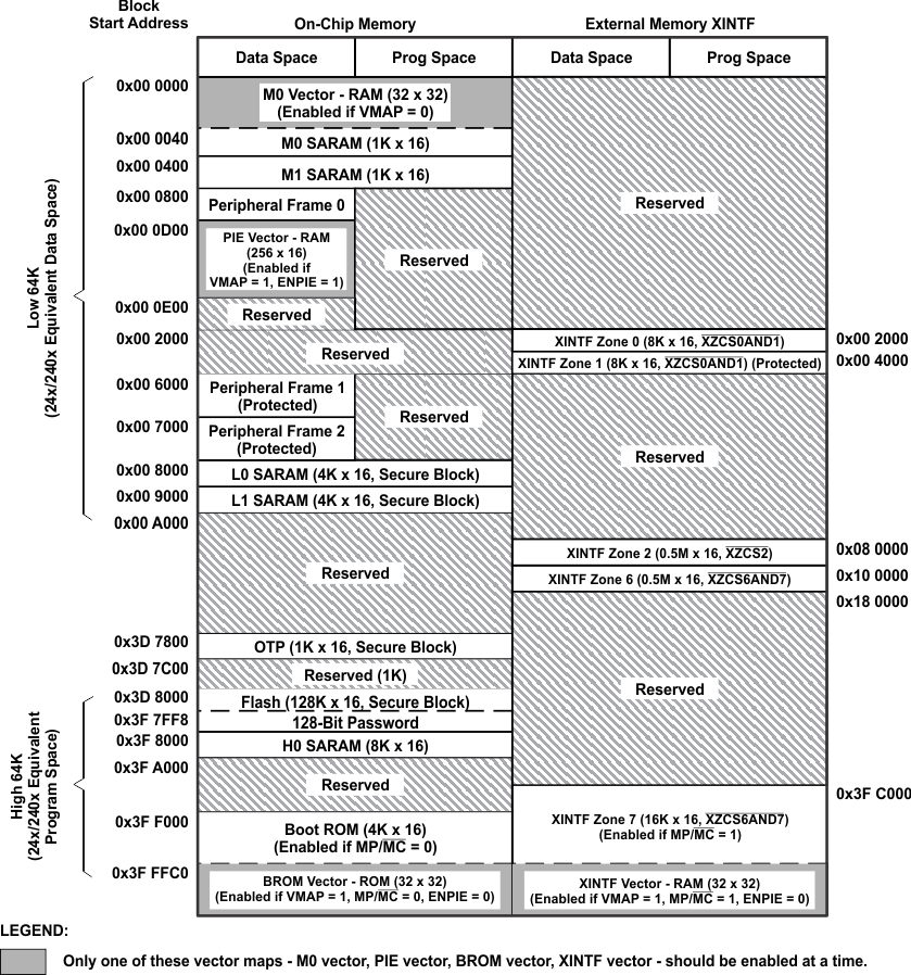
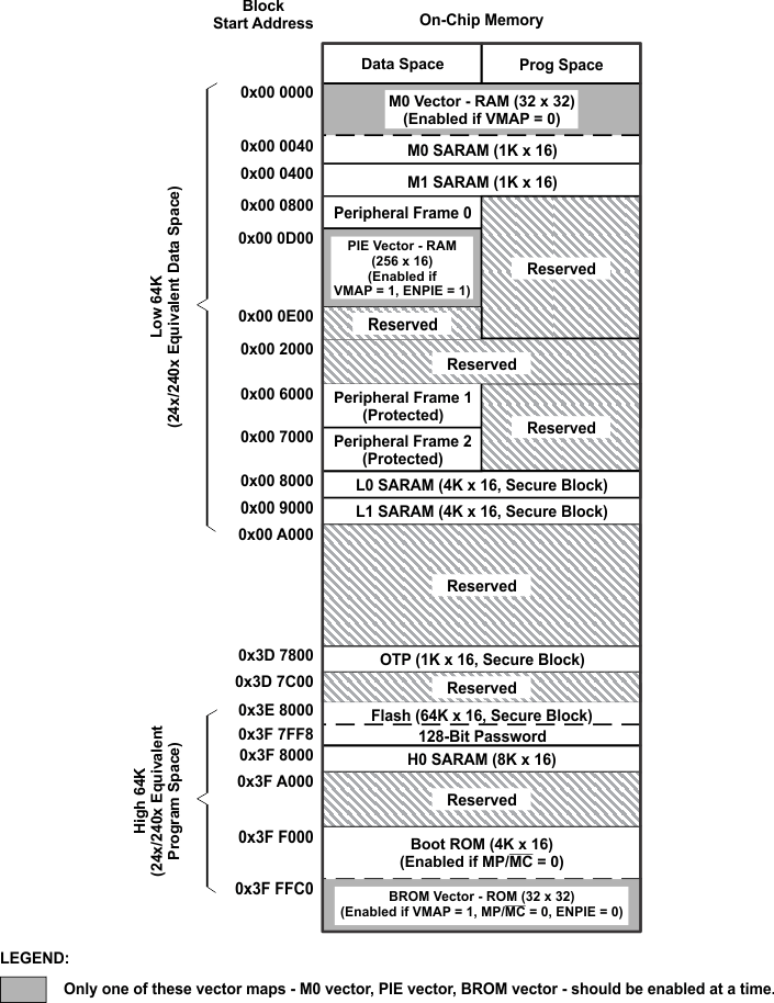
The “Low 64K” of the memory address range maps into the data space of the 240x. The “High 64K” of the memory address range maps into the program space of the 24x/240x. 24x/240x-compatible code will execute only from the “High 64K”memory area. Hence, the top 32K of Flash and H0 SARAM block can be used to run 24x/240x-compatible code (if MP/MC mode is low) or, on the F2812, code can be executed from XINTF Zone 7 (if MP/MC mode is high).
The XINTF consists of five independent zones. One zone has its own chip select and the remaining four zones share two chip selects. Each zone can be programmed with its own timing (wait states) and to either sample or ignore external ready signal. This makes interfacing to external peripherals easy and glueless.
NOTE
The chip selects of XINTF Zone 0 and Zone 1 are merged into a single chip select (XZCS0AND1); and the chip selects of XINTF Zone 6 and Zone 7 are merged into a single chip select (XZCS6AND7). See Section 6.6, External Interface, XINTF (F2812 only), for details.
Peripheral Frame 1, Peripheral Frame 2, and XINTF Zone 1 are grouped together to enable these blocks to be “write/read peripheral block protected”. The “protected” mode ensures that all accesses to these blocks happen as written. Because of the C28x pipeline, a write immediately followed by a read, to different memory locations, will appear in reverse order on the memory bus of the CPU. This can cause problems in certain peripheral applications where the user expected the write to occur first (as written). The C28x CPU supports a block protection mode where a region of memory can be protected to make sure that operations occur as written (the penalty is extra cycles that are added to align the operations). This mode is programmable and, by default, it will protect the selected zones.
On the F2812, at reset, XINTF Zone 7 is accessed if the XMP/MC pin is pulled high. This signal selects microprocessor or microcomputer mode of operation. In microprocessor mode, Zone 7 is mapped to high memory such that the vector table is fetched externally. The Boot ROM is disabled in this mode. In microcomputer mode, Zone 7 is disabled such that the vectors are fetched from Boot ROM. This allows the user to either boot from on-chip memory or from off-chip memory. The state of the XMP/MC signal on reset is stored in an MP/MC mode bit in the XINTCNF2 register. The user can change this mode in software and hence control the mapping of Boot ROM and XINTF Zone 7. No other memory blocks are affected by XMP/MC.
I/O space is not supported on the F2812 XINTF.
The wait states for the various spaces in the memory map area are listed in Table 6-17.
Table 6-17 Wait States
| AREA | WAIT-STATES | COMMENTS |
|---|---|---|
| M0 and M1 SARAMs | 0-wait | Fixed |
| Peripheral Frame 0 | 0-wait | Fixed |
| Peripheral Frame 1 | 0-wait (writes)
2-wait (reads) |
Fixed |
| Peripheral Frame 2 | 0-wait (writes)
2-wait (reads) |
Fixed |
| L0 and L1 SARAMs | 0-wait | Fixed |
| OTP | Programmable,
1-wait minimum |
Programmed via the Flash registers. 1-wait-state operation is possible at a reduced CPU frequency. See Section 6.1.6, Flash, for more information. |
| Flash | Programmable,
0-wait minimum |
Programmed via the Flash registers. 0-wait-state operation is possible at reduced CPU frequency. The CSM password locations are hardwired for 16 wait states. See Section 6.1.6, Flash, for more information. |
| H0 SARAM | 0-wait | Fixed |
| Boot-ROM | 1-wait | Fixed |
| XINTF | Programmable,
1-wait minimum |
Programmed via the XINTF registers.
Cycles can be extended by external memory or peripheral. 0-wait operation is not possible. |