ZHCS894U April 2001 – July 2019 TMS320F2810 , TMS320F2811 , TMS320F2812
PRODUCTION DATA.
- 1器件概述
- 2修订历史记录
- 3Device Comparison
- 4Terminal Configuration and Functions
-
5Specifications
- 5.1 Absolute Maximum Ratings
- 5.2 ESD Ratings – Commercial
- 5.3 ESD Ratings – Automotive
- 5.4 Recommended Operating Conditions
- 5.5 Power Consumption Summary
- 5.6 Electrical Characteristics
- 5.7 Thermal Resistance Characteristics for 179-Ball ZHH Package
- 5.8 Thermal Resistance Characteristics for 179-Ball GHH Package
- 5.9 Thermal Resistance Characteristics for 176-Pin PGF Package
- 5.10 Thermal Resistance Characteristics for 128-Pin PBK Package
- 5.11 Thermal Design Considerations
- 5.12
Timing and Switching Characteristics
- 5.12.1 Timing Parameter Symbology
- 5.12.2 Power Supply Sequencing
- 5.12.3 Reset Timing
- 5.12.4 Clock Specifications
- 5.12.5
Peripherals
- 5.12.5.1 General-Purpose Input/Output (GPIO) – Output Timing
- 5.12.5.2 General-Purpose Input/Output (GPIO) – Input Timing
- 5.12.5.3 Event Manager Interface
- 5.12.5.4 Low-Power Mode Wakeup Timing
- 5.12.5.5 Serial Peripheral Interface (SPI) Master Mode Timing
- 5.12.5.6 Serial Peripheral Interface (SPI) Slave Mode Timing
- 5.12.5.7 External Interface (XINTF) Timing
- 5.12.5.8 XINTF Signal Alignment to XCLKOUT
- 5.12.5.9 External Interface Read Timing
- 5.12.5.10 External Interface Write Timing
- 5.12.5.11
External Interface Ready-on-Read Timing With One External Wait State
- Table 5-31 External Memory Interface Read Switching Characteristics (Ready-on-Read, 1 Wait State)
- Table 5-32 External Memory Interface Read Timing Requirements (Ready-on-Read, 1 Wait State)
- Table 5-33 Synchronous XREADY Timing Requirements (Ready-on-Read, 1 Wait State)
- Table 5-34 Asynchronous XREADY Timing Requirements (Ready-on-Read, 1 Wait State)
- 5.12.5.12 External Interface Ready-on-Write Timing With One External Wait State
- 5.12.5.13 XHOLD and XHOLDA
- 5.12.5.14 XHOLD/XHOLDA Timing
- 5.12.5.15
On-Chip Analog-to-Digital Converter
- Table 5-40 ADC Absolute Maximum Ratings Over Recommended Operating Conditions (Unless Otherwise Noted)
- Table 5-41 ADC Electrical Characteristics Over Recommended Operating Conditions (Unless Otherwise Noted)—AC Specifications
- Table 5-42 ADC Electrical Characteristics Over Recommended Operating Conditions (Unless Otherwise Noted)—DC Specifications
- 5.12.5.15.1 Current Consumption for Different ADC Configurations
- 5.12.5.15.2 ADC Power-Up Control Bit Timing
- 5.12.5.15.3 Detailed Description
- 5.12.5.15.4 Sequential Sampling Mode (Single-Channel) (SMODE = 0)
- 5.12.5.15.5 Simultaneous Sampling Mode (Dual-Channel) (SMODE = 1)
- 5.12.5.15.6 Definitions of Specifications and Terminology
- 5.12.5.16
Multichannel Buffered Serial Port (McBSP) Timing
- 5.12.5.16.1 McBSP Transmit and Receive Timing
- 5.12.5.16.2
McBSP as SPI Master or Slave Timing
- Table 5-49 McBSP as SPI Master or Slave Timing Requirements (CLKSTP = 10b, CLKXP = 0)
- Table 5-50 McBSP as SPI Master or Slave Switching Characteristics (CLKSTP = 10b, CLKXP = 0)
- Table 5-51 McBSP as SPI Master or Slave Timing Requirements (CLKSTP = 11b, CLKXP = 0)
- Table 5-52 McBSP as SPI Master or Slave Switching Characteristics (CLKSTP = 11b, CLKXP = 0)
- Table 5-53 McBSP as SPI Master or Slave Timing Requirements (CLKSTP = 10b, CLKXP = 1)
- Table 5-54 McBSP as SPI Master or Slave Switching Characteristics (CLKSTP = 10b, CLKXP = 1)
- Table 5-55 McBSP as SPI Master or Slave Timing Requirements (CLKSTP = 11b, CLKXP = 1)
- Table 5-56 McBSP as SPI Master or Slave Switching Characteristics (CLKSTP = 11b, CLKXP = 1)
- 5.12.6 Emulator Connection Without Signal Buffering for the DSP
- 5.12.7 Interrupt Timing
- 5.12.8 Flash Timing
-
6Detailed Description
- 6.1
Brief Descriptions
- 6.1.1 C28x CPU
- 6.1.2 Memory Bus (Harvard Bus Architecture)
- 6.1.3 Peripheral Bus
- 6.1.4 Real-Time JTAG and Analysis
- 6.1.5 External Interface (XINTF) (F2812 Only)
- 6.1.6 Flash
- 6.1.7 M0, M1 SARAMs
- 6.1.8 L0, L1, H0 SARAMs
- 6.1.9 Boot ROM
- 6.1.10 Security
- 6.1.11 Peripheral Interrupt Expansion (PIE) Block
- 6.1.12 External Interrupts (XINT1, XINT2, XINT13, XNMI)
- 6.1.13 Oscillator and PLL
- 6.1.14 Watchdog
- 6.1.15 Peripheral Clocking
- 6.1.16 Low-Power Modes
- 6.1.17 Peripheral Frames 0, 1, 2 (PFn)
- 6.1.18 General-Purpose Input/Output (GPIO) Multiplexer
- 6.1.19 32-Bit CPU-Timers (0, 1, 2)
- 6.1.20 Control Peripherals
- 6.1.21 Serial Port Peripherals
- 6.2
Peripherals
- 6.2.1 32-Bit CPU-Timers 0/1/2
- 6.2.2
Event Manager Modules (EVA, EVB)
- 6.2.2.1 General-Purpose (GP) Timers
- 6.2.2.2 Full-Compare Units
- 6.2.2.3 Programmable Deadband Generator
- 6.2.2.4 PWM Waveform Generation
- 6.2.2.5 Double Update PWM Mode
- 6.2.2.6 PWM Characteristics
- 6.2.2.7 Capture Unit
- 6.2.2.8 Quadrature-Encoder Pulse (QEP) Circuit
- 6.2.2.9 External ADC Start-of-Conversion
- 6.2.3 Enhanced Analog-to-Digital Converter (ADC) Module
- 6.2.4 Enhanced Controller Area Network (eCAN) Module
- 6.2.5 Multichannel Buffered Serial Port (McBSP) Module
- 6.2.6 Serial Communications Interface (SCI) Module
- 6.2.7 Serial Peripheral Interface (SPI) Module
- 6.2.8 GPIO MUX
- 6.3 Memory Maps
- 6.4 Register Map
- 6.5 Device Emulation Registers
- 6.6 External Interface, XINTF (F2812 Only)
- 6.7 Interrupts
- 6.8 System Control
- 6.9 OSC and PLL Block
- 6.10 PLL-Based Clock Module
- 6.11 External Reference Oscillator Clock Option
- 6.12 Watchdog Block
- 6.13 Low-Power Modes Block
- 6.1
Brief Descriptions
- 7Applications, Implementation, and Layout
- 8器件和文档支持
- 9机械、封装和可订购信息
封装选项
请参考 PDF 数据表获取器件具体的封装图。
机械数据 (封装 | 引脚)
- PBK|128
散热焊盘机械数据 (封装 | 引脚)
- PBK|128
订购信息
6.7 Interrupts
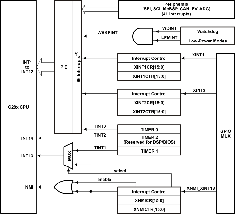
Figure 6-17 shows how the various interrupt sources are multiplexed within the F281x devices.

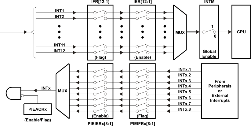
Eight PIE block interrupts are grouped into one CPU interrupt. In total, 12 CPU interrupt groups, with 8 interrupts per group equals 96 possible interrupts. On the F281x, 45 of these are used by peripherals as shown in Table 6-24.
The TRAP #VectorNumber instruction transfers program control to the interrupt service routine corresponding to the vector specified. TRAP #0 attempts to transfer program control to the address pointed to by the reset vector. The PIE vector table does not, however, include a reset vector. Therefore, TRAP #0 should not be used when the PIE is enabled. Doing so will result in undefined behavior.
When the PIE is enabled, TRAP #1 through TRAP #12 will transfer program control to the interrupt service routine corresponding to the first vector within the PIE group. For example: TRAP #1 fetches the vector from INT1.1, TRAP #2 fetches the vector from INT2.1 and so forth.
 Figure 6-18 Multiplexing of Interrupts Using the PIE Block
 Table 6-24 PIE Peripheral Interrupts(1)
| CPU
INTERRUPTS |
PIE INTERRUPTS | |||||||
|---|---|---|---|---|---|---|---|---|
| INTx.8 | INTx.7 | INTx.6 | INTx.5 | INTx.4 | INTx.3 | INTx.2 | INTx.1 | |
| INT1 | WAKEINT
(LPM/WD) |
TINT0
(TIMER 0) |
ADCINT
(ADC) |
XINT2 | XINT1 | Reserved | PDPINTB
(EV-B) |
PDPINTA
(EV-A) |
| INT2 | Reserved | T1OFINT
(EV-A) |
T1UFINT
(EV-A) |
T1CINT
(EV-A) |
T1PINT
(EV-A) |
CMP3INT
(EV-A) |
CMP2INT
(EV-A) |
CMP1INT
(EV-A) |
| INT3 | Reserved | CAPINT3
(EV-A) |
CAPINT2
(EV-A) |
CAPINT1
(EV-A) |
T2OFINT
(EV-A) |
T2UFINT
(EV-A) |
T2CINT
(EV-A) |
T2PINT
(EV-A) |
| INT4 | Reserved | T3OFINT
(EV-B) |
T3UFINT
(EV-B) |
T3CINT
(EV-B) |
T3PINT
(EV-B) |
CMP6INT
(EV-B) |
CMP5INT
(EV-B) |
CMP4INT
(EV-B) |
| INT5 | Reserved | CAPINT6
(EV-B) |
CAPINT5
(EV-B) |
CAPINT4
(EV-B) |
T4OFINT
(EV-B) |
T4UFINT
(EV-B) |
T4CINT
(EV-B) |
T4PINT
(EV-B) |
| INT6 | Reserved | Reserved | MXINT
(McBSP) |
MRINT
(McBSP) |
Reserved | Reserved | SPITXINTA
(SPI) |
SPIRXINTA
(SPI) |
| INT7 | Reserved | Reserved | Reserved | Reserved | Reserved | Reserved | Reserved | Reserved |
| INT8 | Reserved | Reserved | Reserved | Reserved | Reserved | Reserved | Reserved | Reserved |
| INT9 | Reserved | Reserved | ECAN1INT
(CAN) |
ECAN0INT
(CAN) |
SCITXINTB
(SCI-B) |
SCIRXINTB
(SCI-B) |
SCITXINTA
(SCI-A) |
SCIRXINTA
(SCI-A) |
| INT10 | Reserved | Reserved | Reserved | Reserved | Reserved | Reserved | Reserved | Reserved |
| INT11 | Reserved | Reserved | Reserved | Reserved | Reserved | Reserved | Reserved | Reserved |
| INT12 | Reserved | Reserved | Reserved | Reserved | Reserved | Reserved | Reserved | Reserved |
To summarize, there are two safe cases when the reserved interrupts could be used as software interrupts:
- No peripheral within the group is asserting interrupts.
- No peripheral interrupts are assigned to the group (example PIE group 12).
Table 6-25 PIE Configuration and Control Registers(1)
| NAME | ADDRESS | SIZE (x16) | DESCRIPTION |
|---|---|---|---|
| PIECTRL | 0x0000 0CE0 | 1 | PIE, Control Register |
| PIEACK | 0x0000 0CE1 | 1 | PIE, Acknowledge Register |
| PIEIER1 | 0x0000 0CE2 | 1 | PIE, INT1 Group Enable Register |
| PIEIFR1 | 0x0000 0CE3 | 1 | PIE, INT1 Group Flag Register |
| PIEIER2 | 0x0000 0CE4 | 1 | PIE, INT2 Group Enable Register |
| PIEIFR2 | 0x0000 0CE5 | 1 | PIE, INT2 Group Flag Register |
| PIEIER3 | 0x0000 0CE6 | 1 | PIE, INT3 Group Enable Register |
| PIEIFR3 | 0x0000 0CE7 | 1 | PIE, INT3 Group Flag Register |
| PIEIER4 | 0x0000 0CE8 | 1 | PIE, INT4 Group Enable Register |
| PIEIFR4 | 0x0000 0CE9 | 1 | PIE, INT4 Group Flag Register |
| PIEIER5 | 0x0000 0CEA | 1 | PIE, INT5 Group Enable Register |
| PIEIFR5 | 0x0000 0CEB | 1 | PIE, INT5 Group Flag Register |
| PIEIER6 | 0x0000 0CEC | 1 | PIE, INT6 Group Enable Register |
| PIEIFR6 | 0x0000 0CED | 1 | PIE, INT6 Group Flag Register |
| PIEIER7 | 0x0000 0CEE | 1 | PIE, INT7 Group Enable Register |
| PIEIFR7 | 0x0000 0CEF | 1 | PIE, INT7 Group Flag Register |
| PIEIER8 | 0x0000 0CF0 | 1 | PIE, INT8 Group Enable Register |
| PIEIFR8 | 0x0000 0CF1 | 1 | PIE, INT8 Group Flag Register |
| PIEIER9 | 0x0000 0CF2 | 1 | PIE, INT9 Group Enable Register |
| PIEIFR9 | 0x0000 0CF3 | 1 | PIE, INT9 Group Flag Register |
| PIEIER10 | 0x0000 0CF4 | 1 | PIE, INT10 Group Enable Register |
| PIEIFR10 | 0x0000 0CF5 | 1 | PIE, INT10 Group Flag Register |
| PIEIER11 | 0x0000 0CF6 | 1 | PIE, INT11 Group Enable Register |
| PIEIFR11 | 0x0000 0CF7 | 1 | PIE, INT11 Group Flag Register |
| PIEIER12 | 0x0000 0CF8 | 1 | PIE, INT12 Group Enable Register |
| PIEIFR12 | 0x0000 0CF9 | 1 | PIE, INT12 Group Flag Register |
| Reserved | 0x0000 0CFA – 0x0000 0CFF | 6 | Reserved |