ZHCSHE0 December 2017 TMS320F28377D-EP
PRODUCTION DATA.
- 1器件概述
- 2Revision History
- 3Terminal Configuration and Functions
-
4Specifications
- 4.1 Absolute Maximum Ratings
- 4.2 ESD Ratings
- 4.3 Recommended Operating Conditions
- 4.4 Power Consumption Summary
- 4.5 Electrical Characteristics
- 4.6 Thermal Resistance Characteristics
- 4.7
System
- 4.7.1 Power Sequencing
- 4.7.2 Reset Timing
- 4.7.3
Clock Specifications
- 4.7.3.1 Clock Sources
- 4.7.3.2 Clock Frequencies, Requirements, and Characteristics
- 4.7.3.3 Input Clocks and PLLs
- 4.7.3.4 Crystal Oscillator
- 4.7.3.5 Internal Oscillators
- 4.7.4 Flash Parameters
- 4.7.5 Emulation/JTAG
- 4.7.6 GPIO Electrical Data and Timing
- 4.7.7 Interrupts
- 4.7.8
Low-Power Modes
- 4.7.8.1 Clock-Gating Low-Power Modes
- 4.7.8.2 Power-Gating Low-Power Modes
- 4.7.8.3
Low-Power Mode Wakeup Timing
- Table 4-29 IDLE Mode Timing Requirements
- Table 4-30 IDLE Mode Switching Characteristics
- Table 4-31 STANDBY Mode Timing Requirements
- Table 4-32 STANDBY Mode Switching Characteristics
- Table 4-33 HALT Mode Timing Requirements
- Table 4-34 HALT Mode Switching Characteristics
- Table 4-35 HIBERNATE Mode Timing Requirements
- Table 4-36 HIBERNATE Mode Switching Characteristics
- 4.7.9 External Memory Interface (EMIF)
- 4.8
Analog Peripherals
- 4.8.1
Analog-to-Digital Converter (ADC)
- 4.8.1.1
ADC Electrical Data and Timing
- Table 4-41 ADC Operating Conditions (16-Bit Differential Mode)
- Table 4-42 ADC Characteristics (16-Bit Differential Mode)
- Table 4-43 ADC Operating Conditions (12-Bit Single-Ended Mode)
- Table 4-44 ADC Characteristics (12-Bit Single-Ended Mode)
- Table 4-45 ADCEXTSOC Timing Requirements
- 4.8.1.1.1 ADC Input Models
- 4.8.1.1.2 ADC Timing Diagrams
- 4.8.1.2 Temperature Sensor Electrical Data and Timing
- 4.8.1.1
ADC Electrical Data and Timing
- 4.8.2 Comparator Subsystem (CMPSS)
- 4.8.3 Buffered Digital-to-Analog Converter (DAC)
- 4.8.1
Analog-to-Digital Converter (ADC)
- 4.9
Control Peripherals
- 4.9.1 Enhanced Capture (eCAP)
- 4.9.2 Enhanced Pulse Width Modulator (ePWM)
- 4.9.3 Enhanced Quadrature Encoder Pulse (eQEP)
- 4.9.4 High-Resolution Pulse Width Modulator (HRPWM)
- 4.9.5 Sigma-Delta Filter Module (SDFM)
- 4.10
Communications Peripherals
- 4.10.1 Controller Area Network (CAN)
- 4.10.2 Inter-Integrated Circuit (I2C)
- 4.10.3
Multichannel Buffered Serial Port (McBSP)
- 4.10.3.1
McBSP Electrical Data and Timing
- 4.10.3.1.1 McBSP Transmit and Receive Timing
- 4.10.3.1.2
McBSP as SPI Master or Slave Timing
- Table 4-69 McBSP as SPI Master or Slave Timing Requirements (CLKSTP = 10b, CLKXP = 0)
- Table 4-70 McBSP as SPI Master or Slave Switching Characteristics (CLKSTP = 10b, CLKXP = 0)
- Table 4-71 McBSP as SPI Master or Slave Timing Requirements (CLKSTP = 11b, CLKXP = 0)
- Table 4-72 McBSP as SPI Master or Slave Switching Characteristics (CLKSTP = 11b, CLKXP = 0)
- Table 4-73 McBSP as SPI Master or Slave Timing Requirements (CLKSTP = 10b, CLKXP = 1)
- Table 4-74 McBSP as SPI Master or Slave Switching Characteristics (CLKSTP = 10b, CLKXP = 1)
- Table 4-75 McBSP as SPI Master or Slave Timing Requirements (CLKSTP = 11b, CLKXP = 1)
- Table 4-76 McBSP as SPI Master or Slave Switching Characteristics (CLKSTP = 11b, CLKXP = 1)
- 4.10.3.1
McBSP Electrical Data and Timing
- 4.10.4 Serial Communications Interface (SCI)
- 4.10.5 Serial Peripheral Interface (SPI)
- 4.10.6 Universal Serial Bus (USB) Controller
- 4.10.7 Universal Parallel Port (uPP) Interface
-
5Detailed Description
- 5.1 Overview
- 5.2 Functional Block Diagram
- 5.3 Memory
- 5.4 Identification
- 5.5 Bus Architecture – Peripheral Connectivity
- 5.6 C28x Processor
- 5.7 Control Law Accelerator
- 5.8 Direct Memory Access
- 5.9 Interprocessor Communication Module
- 5.10 Boot ROM and Peripheral Booting
- 5.11 Dual Code Security Module
- 5.12 Timers
- 5.13 Nonmaskable Interrupt With Watchdog Timer (NMIWD)
- 5.14 Watchdog
- 5.15 Configurable Logic Block (CLB)
- 6Applications, Implementation, and Layout
- 7器件和文档支持
- 8机械封装和可订购信息
封装选项
机械数据 (封装 | 引脚)
散热焊盘机械数据 (封装 | 引脚)
- PTP|176
订购信息
Table 4-52 Comparator Electrical Characteristics
over recommended operating conditions (unless otherwise noted)| PARAMETER | TEST CONDITIONS | MIN | TYP | MAX | UNIT |
|---|---|---|---|---|---|
| Power-up time (from COMPCTL[COMPDACE] to comparator ready) | 10 | µs | |||
| Comparator input (CMPINxx) range | 0 | VDDA | V | ||
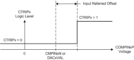
| Input referred offset error | –20 | 20 | mV | ||
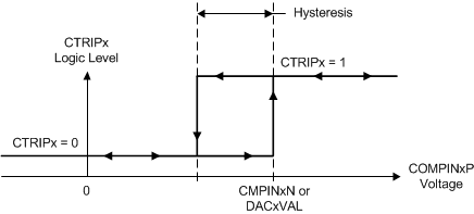
| Hysteresis(1) | 1x | 12 | CMPSS DAC LSB | ||
| 2x | 24 | ||||
| 3x | 36 | ||||
| 4x | 48 | ||||
| Response time (delay from CMPINx input change to output on ePWM X-BAR or Output X-BAR) | Step response | 21 | 60 | ns | |
| Ramp response (1.65 V/µs) | 26 | ||||
| Ramp response (8.25 mV/µs) | 30 |
NOTE
The CMPSS inputs must be kept below VDDA + 0.3 V to ensure proper functional operation. If a CMPSS input exceeds this level, an internal blocking circuit will isolate the internal comparator from the external pin until the external pin voltage returns below VDDA + 0.3 V. During this time, the internal comparator input will be floating and can decay below VDDA within approximately 0.5 µs. After this time, the comparator could begin to output an incorrect result depending on the value of the other comparator input.
 Figure 4-38 CMPSS Comparator Input Referred Offset
 Figure 4-39 CMPSS Comparator Hysteresis
Table 4-53 shows the CMPSS DAC static electrical characteristics. Figure 4-40 shows the CMPSS DAC static offset. Figure 4-41 shows the CMPSS DAC static gain. Figure 4-42 shows the CMPSS DAC static linearity.