ZHCSHE0 December   2017 TMS320F28377D-EP

PRODUCTION DATA.  

  1. 1器件概述
    1. 1.1 特性
    2. 1.2 应用
    3. 1.3 说明
    4. 1.4 功能框图
  2. 2Revision History
  3. 3Terminal Configuration and Functions
    1. 3.1 Pin Diagrams
    2. 3.2 Signal Descriptions
      1. Table 3-1 Signal Descriptions
    3. 3.3 Pins With Internal Pullup and Pulldown
    4. 3.4 Pin Multiplexing
      1. 3.4.1 GPIO Muxed Pins
      2. 3.4.2 Input X-BAR
      3. 3.4.3 Output X-BAR and ePWM X-BAR
      4. 3.4.4 USB Pin Muxing
      5. 3.4.5 High-Speed SPI Pin Muxing
    5. 3.5 Connections for Unused Pins
  4. 4Specifications
    1. 4.1  Absolute Maximum Ratings
    2. 4.2  ESD Ratings
    3. 4.3  Recommended Operating Conditions
    4. 4.4  Power Consumption Summary
      1. Table 4-1 Device Current Consumption at 200-MHz SYSCLK
      2. 4.4.1      Current Consumption Graphs
      3. 4.4.2      Reducing Current Consumption
    5. 4.5  Electrical Characteristics
    6. 4.6  Thermal Resistance Characteristics
      1. 4.6.1 GWT Package
      2. 4.6.2 PTP Package
    7. 4.7  System
      1. 4.7.1 Power Sequencing
        1. Table 4-3 Supply Ramp Rate
      2. 4.7.2 Reset Timing
        1. 4.7.2.1 Reset Sources
        2. 4.7.2.2 Reset Electrical Data and Timing
          1. Table 4-4 Reset (XRS) Timing Requirements
          2. Table 4-5 Reset (XRS) Switching Characteristics
      3. 4.7.3 Clock Specifications
        1. 4.7.3.1 Clock Sources
        2. 4.7.3.2 Clock Frequencies, Requirements, and Characteristics
          1. 4.7.3.2.1 Input Clock Frequency and Timing Requirements, PLL Lock Times
            1. Table 4-7   Input Clock Frequency
            2. Table 4-8   X1 Input Level Characteristics When Using an External Clock Source (Not a Crystal)
            3. Table 4-9   X1 Timing Requirements
            4. Table 4-10 AUXCLKIN Timing Requirements
            5. Table 4-11 PLL Lock Times
          2. 4.7.3.2.2 Internal Clock Frequencies
            1. Table 4-12 Internal Clock Frequencies
          3. 4.7.3.2.3 Output Clock Frequency and Switching Characteristics
            1. Table 4-13 Output Clock Frequency
            2. Table 4-14 XCLKOUT Switching Characteristics (PLL Bypassed or Enabled)
        3. 4.7.3.3 Input Clocks and PLLs
        4. 4.7.3.4 Crystal Oscillator
          1. Table 4-15 Crystal Oscillator Parameters
          2. Table 4-17 Crystal Oscillator Electrical Characteristics
        5. 4.7.3.5 Internal Oscillators
          1. Table 4-18 Internal Oscillator Electrical Characteristics
      4. 4.7.4 Flash Parameters
        1. Table 4-20 Flash Parameters
      5. 4.7.5 Emulation/JTAG
        1. 4.7.5.1 JTAG Electrical Data and Timing
          1. Table 4-21 JTAG Timing Requirements
          2. Table 4-22 JTAG Switching Characteristics
      6. 4.7.6 GPIO Electrical Data and Timing
        1. 4.7.6.1 GPIO - Output Timing
          1. Table 4-23 General-Purpose Output Switching Characteristics
        2. 4.7.6.2 GPIO - Input Timing
          1. Table 4-24 General-Purpose Input Timing Requirements
        3. 4.7.6.3 Sampling Window Width for Input Signals
      7. 4.7.7 Interrupts
        1. 4.7.7.1 External Interrupt (XINT) Electrical Data and Timing
          1. Table 4-25 External Interrupt Timing Requirements
          2. Table 4-26 External Interrupt Switching Characteristics
      8. 4.7.8 Low-Power Modes
        1. 4.7.8.1 Clock-Gating Low-Power Modes
        2. 4.7.8.2 Power-Gating Low-Power Modes
        3. 4.7.8.3 Low-Power Mode Wakeup Timing
          1. Table 4-29 IDLE Mode Timing Requirements
          2. Table 4-30 IDLE Mode Switching Characteristics
          3. Table 4-31 STANDBY Mode Timing Requirements
          4. Table 4-32 STANDBY Mode Switching Characteristics
          5. Table 4-33 HALT Mode Timing Requirements
          6. Table 4-34 HALT Mode Switching Characteristics
          7. Table 4-35 HIBERNATE Mode Timing Requirements
          8. Table 4-36 HIBERNATE Mode Switching Characteristics
      9. 4.7.9 External Memory Interface (EMIF)
        1. 4.7.9.1 Asynchronous Memory Support
        2. 4.7.9.2 Synchronous DRAM Support
        3. 4.7.9.3 EMIF Electrical Data and Timing
          1. 4.7.9.3.1 Asynchronous RAM
            1. Table 4-37 EMIF Asynchronous Memory Timing Requirements
            2. Table 4-38 EMIF Asynchronous Memory Switching Characteristics
          2. 4.7.9.3.2 Synchronous RAM
            1. Table 4-39 EMIF Synchronous Memory Timing Requirements
            2. Table 4-40 EMIF Synchronous Memory Switching Characteristics
    8. 4.8  Analog Peripherals
      1. 4.8.1 Analog-to-Digital Converter (ADC)
        1. 4.8.1.1 ADC Electrical Data and Timing
          1. Table 4-41 ADC Operating Conditions (16-Bit Differential Mode)
          2. Table 4-42 ADC Characteristics (16-Bit Differential Mode)
          3. Table 4-43 ADC Operating Conditions (12-Bit Single-Ended Mode)
          4. Table 4-44 ADC Characteristics (12-Bit Single-Ended Mode)
          5. Table 4-45 ADCEXTSOC Timing Requirements
          6. 4.8.1.1.1   ADC Input Models
            1. Table 4-46 Single-Ended Input Model Parameters
            2. Table 4-47 Differential Input Model Parameters
          7. 4.8.1.1.2   ADC Timing Diagrams
            1. Table 4-49 ADC Timings in 12-Bit Mode (SYSCLK Cycles)
            2. Table 4-50 ADC Timings in 16-Bit Mode
        2. 4.8.1.2 Temperature Sensor Electrical Data and Timing
          1. Table 4-51 Temperature Sensor Electrical Characteristics
      2. 4.8.2 Comparator Subsystem (CMPSS)
        1. 4.8.2.1 CMPSS Electrical Data and Timing
          1. Table 4-52 Comparator Electrical Characteristics
          2. Table 4-53 CMPSS DAC Static Electrical Characteristics
      3. 4.8.3 Buffered Digital-to-Analog Converter (DAC)
        1. 4.8.3.1 Buffered DAC Electrical Data and Timing
          1. Table 4-54 Buffered DAC Electrical Characteristics
    9. 4.9  Control Peripherals
      1. 4.9.1 Enhanced Capture (eCAP)
        1. 4.9.1.1 eCAP Electrical Data and Timing
          1. Table 4-55 eCAP Timing Requirement
          2. Table 4-56 eCAP Switching Characteristics
      2. 4.9.2 Enhanced Pulse Width Modulator (ePWM)
        1. 4.9.2.1 Control Peripherals Synchronization
        2. 4.9.2.2 ePWM Electrical Data and Timing
          1. Table 4-57 ePWM Timing Requirements
          2. Table 4-58 ePWM Switching Characteristics
          3. 4.9.2.2.1   Trip-Zone Input Timing
            1. Table 4-59 Trip-Zone Input Timing Requirements
        3. 4.9.2.3 External ADC Start-of-Conversion Electrical Data and Timing
          1. Table 4-60 External ADC Start-of-Conversion Switching Characteristics
      3. 4.9.3 Enhanced Quadrature Encoder Pulse (eQEP)
        1. 4.9.3.1 eQEP Electrical Data and Timing
          1. Table 4-61 eQEP Timing Requirements
          2. Table 4-62 eQEP Switching Characteristics
      4. 4.9.4 High-Resolution Pulse Width Modulator (HRPWM)
        1. 4.9.4.1 HRPWM Electrical Data and Timing
          1. Table 4-63 High-Resolution PWM Characteristics
      5. 4.9.5 Sigma-Delta Filter Module (SDFM)
        1. 4.9.5.1 SDFM Electrical Data and Timing
          1. Table 4-64 SDFM Timing Requirements
    10. 4.10 Communications Peripherals
      1. 4.10.1 Controller Area Network (CAN)
      2. 4.10.2 Inter-Integrated Circuit (I2C)
        1. 4.10.2.1 I2C Electrical Data and Timing
          1. Table 4-65 I2C Timing Requirements
          2. Table 4-66 I2C Switching Characteristics
      3. 4.10.3 Multichannel Buffered Serial Port (McBSP)
        1. 4.10.3.1 McBSP Electrical Data and Timing
          1. 4.10.3.1.1 McBSP Transmit and Receive Timing
            1. Table 4-67 McBSP Timing Requirements
            2. Table 4-68 McBSP Switching Characteristics
          2. 4.10.3.1.2 McBSP as SPI Master or Slave Timing
            1. Table 4-69 McBSP as SPI Master or Slave Timing Requirements (CLKSTP = 10b, CLKXP = 0)
            2. Table 4-70 McBSP as SPI Master or Slave Switching Characteristics (CLKSTP = 10b, CLKXP = 0)
            3. Table 4-71 McBSP as SPI Master or Slave Timing Requirements (CLKSTP = 11b, CLKXP = 0)
            4. Table 4-72 McBSP as SPI Master or Slave Switching Characteristics (CLKSTP = 11b, CLKXP = 0)
            5. Table 4-73 McBSP as SPI Master or Slave Timing Requirements (CLKSTP = 10b, CLKXP = 1)
            6. Table 4-74 McBSP as SPI Master or Slave Switching Characteristics (CLKSTP = 10b, CLKXP = 1)
            7. Table 4-75 McBSP as SPI Master or Slave Timing Requirements (CLKSTP = 11b, CLKXP = 1)
            8. Table 4-76 McBSP as SPI Master or Slave Switching Characteristics (CLKSTP = 11b, CLKXP = 1)
      4. 4.10.4 Serial Communications Interface (SCI)
      5. 4.10.5 Serial Peripheral Interface (SPI)
        1. 4.10.5.1 SPI Electrical Data and Timing
          1. 4.10.5.1.1 Non-High-Speed Master Mode Timings
            1. Table 4-77 SPI Master Mode Switching Characteristics (Clock Phase = 0)
            2. Table 4-78 SPI Master Mode Switching Characteristics (Clock Phase = 1)
            3. Table 4-79 SPI Master Mode Timing Requirements
          2. 4.10.5.1.2 Non-High-Speed Slave Mode Timings
            1. Table 4-80 SPI Slave Mode Switching Characteristics
            2. Table 4-81 SPI Slave Mode Timing Requirements
          3. 4.10.5.1.3 High-Speed Master Mode Timings
            1. Table 4-82 SPI High-Speed Master Mode Switching Characteristics (Clock Phase = 0)
            2. Table 4-83 SPI High-Speed Master Mode Switching Characteristics (Clock Phase = 1)
            3. Table 4-84 SPI High-Speed Master Mode Timing Requirements
          4. 4.10.5.1.4 High-Speed Slave Mode Timings
            1. Table 4-85 SPI High-Speed Slave Mode Switching Characteristics
            2. Table 4-86 SPI High-Speed Slave Mode Timing Requirements
      6. 4.10.6 Universal Serial Bus (USB) Controller
        1. 4.10.6.1 USB Electrical Data and Timing
          1. Table 4-87 USB Input Ports DP and DM Timing Requirements
          2. Table 4-88 USB Output Ports DP and DM Switching Characteristics
      7. 4.10.7 Universal Parallel Port (uPP) Interface
        1. 4.10.7.1 uPP Electrical Data and Timing
          1. Table 4-89 uPP Timing Requirements
          2. Table 4-90 uPP Switching Characteristics
  5. 5Detailed Description
    1. 5.1  Overview
    2. 5.2  Functional Block Diagram
    3. 5.3  Memory
      1. 5.3.1 C28x Memory Map
      2. 5.3.2 Flash Memory Map
      3. 5.3.3 EMIF Chip Select Memory Map
      4. 5.3.4 Peripheral Registers Memory Map
      5. 5.3.5 Memory Types
        1. 5.3.5.1 Dedicated RAM (Mx and Dx RAM)
        2. 5.3.5.2 Local Shared RAM (LSx RAM)
        3. 5.3.5.3 Global Shared RAM (GSx RAM)
        4. 5.3.5.4 CPU Message RAM (CPU MSGRAM)
        5. 5.3.5.5 CLA Message RAM (CLA MSGRAM)
    4. 5.4  Identification
    5. 5.5  Bus Architecture – Peripheral Connectivity
    6. 5.6  C28x Processor
      1. 5.6.1 Floating-Point Unit
      2. 5.6.2 Trigonometric Math Unit
      3. 5.6.3 Viterbi, Complex Math, and CRC Unit II (VCU-II)
    7. 5.7  Control Law Accelerator
    8. 5.8  Direct Memory Access
    9. 5.9  Interprocessor Communication Module
    10. 5.10 Boot ROM and Peripheral Booting
      1. 5.10.1 EMU Boot or Emulation Boot
      2. 5.10.2 WAIT Boot Mode
      3. 5.10.3 Get Mode
      4. 5.10.4 Peripheral Pins Used by Bootloaders
    11. 5.11 Dual Code Security Module
    12. 5.12 Timers
    13. 5.13 Nonmaskable Interrupt With Watchdog Timer (NMIWD)
    14. 5.14 Watchdog
    15. 5.15 Configurable Logic Block (CLB)
  6. 6Applications, Implementation, and Layout
    1. 6.1 TI Design or Reference Design
  7. 7器件和文档支持
    1. 7.1 器件和开发支持工具命名规则
    2. 7.2 工具和软件
    3. 7.3 器件命名规则
    4. 7.4 文档支持
    5. 7.5 Community Resources
    6. 7.6 商标
    7. 7.7 静电放电警告
    8. 7.8 出口管制提示
    9. 7.9 术语表
  8. 8机械封装和可订购信息
    1. 8.1 Via Channel
    2. 8.2 封装信息

封装选项

机械数据 (封装 | 引脚)
散热焊盘机械数据 (封装 | 引脚)
订购信息

Universal Parallel Port (uPP) Interface

The uPP interface is a high-speed parallel interface with dedicated data lines and minimal control signals. The uPP interface is designed to interface cleanly with high-speed ADCs or DACs with 8-bit data width. It can also be interconnected with field-programmable gate arrays (FPGAs) or other uPP devices to achieve high-speed digital data transfer. It can operate in receive mode or transmit mode (simplex mode).

The uPP interface includes an internal DMA controller to maximize throughput and minimize CPU overhead during high-speed data transmission. All uPP transactions use internal DMA to feed data to or retrieve data from the I/O channels. Even though there is only one I/O channel, the DMA controller includes two DMA channels to support data interleave mode, in which all DMA resources service a single I/O channel.

On this device, the uPP interface is the dedicated resource for the CPU1 subsystem. CPU1, CPU1.CLA1, and CPU1.DMA have access to this module. Two dedicated 512-byte data RAMs (also known as MSG RAMs) are tightly coupled with the uPP module (one for each, TX and RX). These data RAMs are used to store the bulk of data to avoid frequent interruptions to the CPU. Only CPU1 and CPU1.CLA1 have access to these data RAMs. Figure 4-78 shows the integration of the uPP on this device.
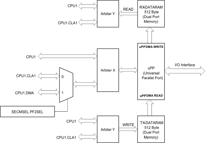
TMS320F28377D-EP Figure_1_spruhm8.gifFigure 4-78 uPP Integration

NOTE

On some TI devices, the uPP module is also called the Radio Peripheral Interface (RPI) module.

The uPP interface supports the following:

  • Mainstream high-speed data converters with parallel conversion interface.
  • Mainstream high-speed streaming interface with frame START indication.
  • Mainstream high-speed streaming interface with data ENABLE indication.
  • Mainstream high-speed streaming interface with synchronization WAIT signal.
  • SDR (single-data-rate) or DDR (double-data-rate, interleaved) interface.
  • Multiplexing of interleaved data in SDR transmit case.
  • Demultiplexing and multiplexing of interleaved data in DDR case.
  • I/O interface clock frequency up to 50 MHz for SDR, and 25 MHz for DDR.
  • Single-channel 8-bit input receive or output transmit mode.
  • Max throughput is 50MB/s for pure read or pure write.
  • Available as a DSP to FPGA general-purpose streaming interface.

Figure 4-79 shows the uPP functional block diagram.
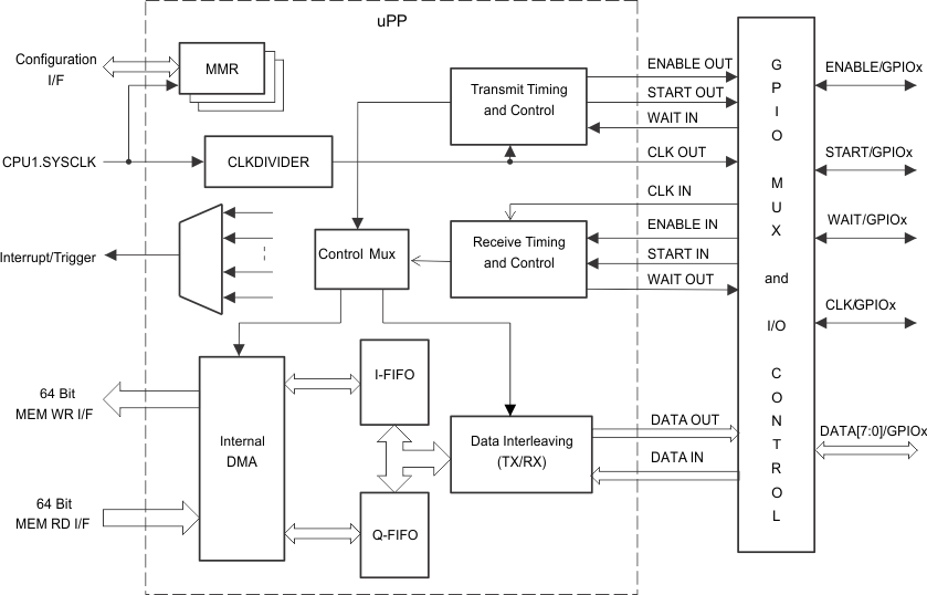
TMS320F28377D-EP Figure_2_spruhm8.gifFigure 4-79 uPP Functional Block Diagram