ZHCSV76A June 2022 – March 2024 TMS570LC4357-SEP
PRODUCTION DATA
- 1
- 1 特性
- 2 应用
- 3 说明
- 4 Device Comparison
-
5 Terminal Configuration and Functions
- 5.1 GWT BGA Package Ball-Map (337 Terminal Grid Array)
- 5.2
Terminal Functions
- 5.2.1
GWT Package
- 5.2.1.1 Multibuffered Analog-to-Digital Converters (MibADC)
- 5.2.1.2 Enhanced High-End Timer Modules (N2HET)
- 5.2.1.3 RAM Trace Port (RTP)
- 5.2.1.4 Enhanced Capture Modules (eCAP)
- 5.2.1.5 Enhanced Quadrature Encoder Pulse Modules (eQEP)
- 5.2.1.6 Enhanced Pulse-Width Modulator Modules (ePWM)
- 5.2.1.7 Data Modification Module (DMM)
- 5.2.1.8 General-Purpose Input / Output (GIO)
- 5.2.1.9 FlexRay Interface Controller (FlexRay)
- 5.2.1.10 Controller Area Network Controllers (DCAN)
- 5.2.1.11 Local Interconnect Network Interface Module (LIN)
- 5.2.1.12 Standard Serial Communication Interface (SCI)
- 5.2.1.13 Inter-Integrated Circuit Interface Module (I2C)
- 5.2.1.14 Multibuffered Serial Peripheral Interface Modules (MibSPI)
- 5.2.1.15 Ethernet Controller
- 5.2.1.16 External Memory Interface (EMIF)
- 5.2.1.17 Embedded Trace Macrocell Interface for Cortex-R5F (ETM-R5)
- 5.2.1.18 System Module Interface
- 5.2.1.19 Clock Inputs and Outputs
- 5.2.1.20 Test and Debug Modules Interface
- 5.2.1.21 Flash Supply and Test Pads
- 5.2.1.22 Supply for Core Logic: 1.2-V Nominal
- 5.2.1.23 Supply for I/O Cells: 3.3-V Nominal
- 5.2.1.24 Ground Reference for All Supplies Except VCCAD
- 5.2.1.25 Other Supplies
- 5.2.2 Multiplexing
- 5.2.1
GWT Package
-
6 Specifications
- 6.1 Absolute Maximum Ratings
- 6.2 ESD Ratings
- 6.3 Power-On Hours (POH)
- 6.4 Recommended Operating Conditions
- 6.5 Switching Characteristics Over Recommended Operating Conditions for Clock Domains
- 6.6 Wait States Required - L2 Memories
- 6.7 Power Consumption Summary
- 6.8 Input/Output Electrical Characteristics Over Recommended Operating Conditions
- 6.9 Thermal Resistance Characteristics for the BGA Package (GWT)
- 6.10 Timing and Switching Characteristics
-
7 System Information and Electrical Specifications
- 7.1 Device Power Domains
- 7.2 Voltage Monitor Characteristics
- 7.3 Power Sequencing and Power-On Reset
- 7.4 Warm Reset (nRST)
- 7.5 Arm Cortex-R5F CPU Information
- 7.6 Clocks
- 7.7 Clock Monitoring
- 7.8 Glitch Filters
- 7.9 Device Memory Map
- 7.10 Flash Memory
- 7.11 L2RAMW (Level 2 RAM Interface Module)
- 7.12 ECC / Parity Protection for Accesses to Peripheral RAMs
- 7.13 On-Chip SRAM Initialization and Testing
- 7.14 External Memory Interface (EMIF)
- 7.15 Vectored Interrupt Manager
- 7.16 ECC Error Event Monitoring and Profiling
- 7.17 DMA Controller
- 7.18 Real-Time Interrupt Module
- 7.19 Error Signaling Module
- 7.20 Reset / Abort / Error Sources
- 7.21 Digital Windowed Watchdog
- 7.22
Debug Subsystem
- 7.22.1 Block Diagram
- 7.22.2 Debug Components Memory Map
- 7.22.3 Embedded Cross Trigger
- 7.22.4 JTAG Identification Code
- 7.22.5 Debug ROM
- 7.22.6 JTAG Scan Interface Timings
- 7.22.7 Advanced JTAG Security Module
- 7.22.8 Embedded Trace Macrocell (ETM-R5)
- 7.22.9 RAM Trace Port (RTP)
- 7.22.10 Data Modification Module (DMM)
- 7.22.11 Boundary Scan Chain
-
8 Peripheral Information and Electrical Specifications
- 8.1
Enhanced Translator PWM Modules (ePWM)
- 8.1.1 ePWM Clocking and Reset
- 8.1.2 Synchronization of ePWMx Time-Base Counters
- 8.1.3 Synchronizing all ePWM Modules to the N2HET1 Module Time Base
- 8.1.4 Phase-Locking the Time-Base Clocks of Multiple ePWM Modules
- 8.1.5 ePWM Synchronization with External Devices
- 8.1.6 ePWM Trip Zones
- 8.1.7 Triggering of ADC Start of Conversion Using ePWMx SOCA and SOCB Outputs
- 8.1.8 Enhanced Translator-Pulse Width Modulator (ePWMx) Electrical Data/Timing
- 8.2 Enhanced Capture Modules (eCAP)
- 8.3 Enhanced Quadrature Encoder (eQEP)
- 8.4 12-bit Multibuffered Analog-to-Digital Converter (MibADC)
- 8.5 General-Purpose Input/Output
- 8.6 Enhanced High-End Timer (N2HET)
- 8.7 FlexRay Interface
- 8.8 Controller Area Network (DCAN)
- 8.9 Local Interconnect Network Interface (LIN)
- 8.10 Serial Communication Interface (SCI)
- 8.11 Inter-Integrated Circuit (I2C)
- 8.12 Multibuffered / Standard Serial Peripheral Interface
- 8.13 Ethernet Media Access Controller
- 8.1
Enhanced Translator PWM Modules (ePWM)
- 9 Applications, Implementation, and Layout
- 10Device and Documentation Support
- 11Revision History
- 12Mechanical, Packaging, and Orderable Information
请参考 PDF 数据表获取器件具体的封装图。
7.22.7 Advanced JTAG Security Module
This device includes an Advanced JTAG Security Module (AJSM), which lets the user limit JTAG access to the device after programming.
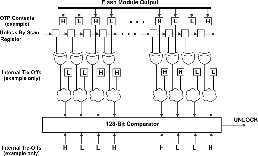
 Figure 7-29 AJSM Unlock
The device is unlocked by default by virtue of a 128-bit visible unlock code programmed in the One-Time Programmable (OTP) address 0xF000 0000.The OTP contents are XOR-ed with the contents of the Unlock-By-Scan register. The outputs of these XOR gates are again combined with a set of secret internal tie-offs. The output of this combinational logic is compared against a secret, hard-wired, 128-bit value. A match asserts the UNLOCK signal, so that the device is now unlocked.
A user can lock the device by changing bits in the visible unlock code from 1 to 0. Changing a 0 to 1 is not possible because the visible unlock code is stored in the OTP flash region. Also, changing all the 128 bits to zeros is not a valid condition and will permanently lock the device.
Once locked, a user can unlock the device by scanning an appropriate value into the Unlock-By-Scan register of the AJSM module. This register is accessible by configuring an IR value of 0b1011 on the AJSM TAP. The value to be scanned is such that the XOR of the OTP contents and the contents of the Unlock-By-Scan register results in the original visible unlock code.
The Unlock-By-Scan register is reset only by asserting power-on reset (nPORRST).
A locked device only permits JTAG accesses to the AJSM scan chain through the Secondary TAP 2 of the ICEPick module. All other secondary TAPs, test TAPs and the boundary scan interface are not accessible in this state.