ZHCSCJ1C February 2014 – June 2016 TMS570LC4357
PRODUCTION DATA.
- 1 器件概述
- 2 修订历史记录
- 3 Device Comparison
-
4 Terminal Configuration and Functions
- 4.1 ZWT BGA Package Ball-Map (337 Terminal Grid Array)
- 4.2
Terminal Functions
- 4.2.1
ZWT Package
- 4.2.1.1 Multibuffered Analog-to-Digital Converters (MibADC)
- 4.2.1.2 Enhanced High-End Timer Modules (N2HET)
- 4.2.1.3 RAM Trace Port (RTP)
- 4.2.1.4 Enhanced Capture Modules (eCAP)
- 4.2.1.5 Enhanced Quadrature Encoder Pulse Modules (eQEP)
- 4.2.1.6 Enhanced Pulse-Width Modulator Modules (ePWM)
- 4.2.1.7 Data Modification Module (DMM)
- 4.2.1.8 General-Purpose Input / Output (GIO)
- 4.2.1.9 FlexRay Interface Controller (FlexRay)
- 4.2.1.10 Controller Area Network Controllers (DCAN)
- 4.2.1.11 Local Interconnect Network Interface Module (LIN)
- 4.2.1.12 Standard Serial Communication Interface (SCI)
- 4.2.1.13 Inter-Integrated Circuit Interface Module (I2C)
- 4.2.1.14 Multibuffered Serial Peripheral Interface Modules (MibSPI)
- 4.2.1.15 Ethernet Controller
- 4.2.1.16 External Memory Interface (EMIF)
- 4.2.1.17 Embedded Trace Macrocell Interface for Cortex-R5F (ETM-R5)
- 4.2.1.18 System Module Interface
- 4.2.1.19 Clock Inputs and Outputs
- 4.2.1.20 Test and Debug Modules Interface
- 4.2.1.21 Flash Supply and Test Pads
- 4.2.1.22 Supply for Core Logic: 1.2-V Nominal
- 4.2.1.23 Supply for I/O Cells: 3.3-V Nominal
- 4.2.1.24 Ground Reference for All Supplies Except VCCAD
- 4.2.1.25 Other Supplies
- 4.2.2 Multiplexing
- 4.2.1
ZWT Package
-
5 Specifications
- 5.1 Absolute Maximum Ratings
- 5.2 ESD Ratings
- 5.3 Power-On Hours (POH)
- 5.4 Device Recommended Operating Conditions
- 5.5 Switching Characteristics over Recommended Operating Conditions for Clock Domains
- 5.6 Wait States Required - L2 Memories
- 5.7 Power Consumption Summary
- 5.8 Input/Output Electrical Characteristics Over Recommended Operating Conditions
- 5.9 Thermal Resistance Characteristics for the BGA Package (ZWT)
- 5.10 Timing and Switching Characteristics
-
6 System Information and Electrical Specifications
- 6.1 Device Power Domains
- 6.2 Voltage Monitor Characteristics
- 6.3 Power Sequencing and Power-On Reset
- 6.4 Warm Reset (nRST)
- 6.5 ARM Cortex-R5F CPU Information
- 6.6 Clocks
- 6.7 Clock Monitoring
- 6.8 Glitch Filters
- 6.9 Device Memory Map
- 6.10 Flash Memory
- 6.11 L2RAMW (Level 2 RAM Interface Module)
- 6.12 ECC / Parity Protection for Accesses to Peripheral RAMs
- 6.13 On-Chip SRAM Initialization and Testing
- 6.14 External Memory Interface (EMIF)
- 6.15 Vectored Interrupt Manager
- 6.16 ECC Error Event Monitoring and Profiling
- 6.17 DMA Controller
- 6.18 Real-Time Interrupt Module
- 6.19 Error Signaling Module
- 6.20 Reset / Abort / Error Sources
- 6.21 Digital Windowed Watchdog
- 6.22
Debug Subsystem
- 6.22.1 Block Diagram
- 6.22.2 Debug Components Memory Map
- 6.22.3 Embedded Cross Trigger
- 6.22.4 JTAG Identification Code
- 6.22.5 Debug ROM
- 6.22.6 JTAG Scan Interface Timings
- 6.22.7 Advanced JTAG Security Module
- 6.22.8 Embedded Trace Macrocell (ETM-R5)
- 6.22.9 RAM Trace Port (RTP)
- 6.22.10 Data Modification Module (DMM)
- 6.22.11 Boundary Scan Chain
-
7 Peripheral Information and Electrical Specifications
- 7.1
Enhanced Translator PWM Modules (ePWM)
- 7.1.1 ePWM Clocking and Reset
- 7.1.2 Synchronization of ePWMx Time-Base Counters
- 7.1.3 Synchronizing all ePWM Modules to the N2HET1 Module Time Base
- 7.1.4 Phase-Locking the Time-Base Clocks of Multiple ePWM Modules
- 7.1.5 ePWM Synchronization with External Devices
- 7.1.6 ePWM Trip Zones
- 7.1.7 Triggering of ADC Start of Conversion Using ePWMx SOCA and SOCB Outputs
- 7.1.8 Enhanced Translator-Pulse Width Modulator (ePWMx) Electrical Data/Timing
- 7.2 Enhanced Capture Modules (eCAP)
- 7.3 Enhanced Quadrature Encoder (eQEP)
- 7.4 12-bit Multibuffered Analog-to-Digital Converter (MibADC)
- 7.5 General-Purpose Input/Output
- 7.6 Enhanced High-End Timer (N2HET)
- 7.7 FlexRay Interface
- 7.8 Controller Area Network (DCAN)
- 7.9 Local Interconnect Network Interface (LIN)
- 7.10 Serial Communication Interface (SCI)
- 7.11 Inter-Integrated Circuit (I2C)
- 7.12 Multibuffered / Standard Serial Peripheral Interface
- 7.13 Ethernet Media Access Controller
- 7.1
Enhanced Translator PWM Modules (ePWM)
- 8 Applications, Implementation, and Layout
- 9 Device and Documentation Support
- 10Mechanical Data
7 Peripheral Information and Electrical Specifications
7.1 Enhanced Translator PWM Modules (ePWM)
Figure 7-1 shows the connections between the seven ePWM modules (ePWM1–ePWM7) on the device.
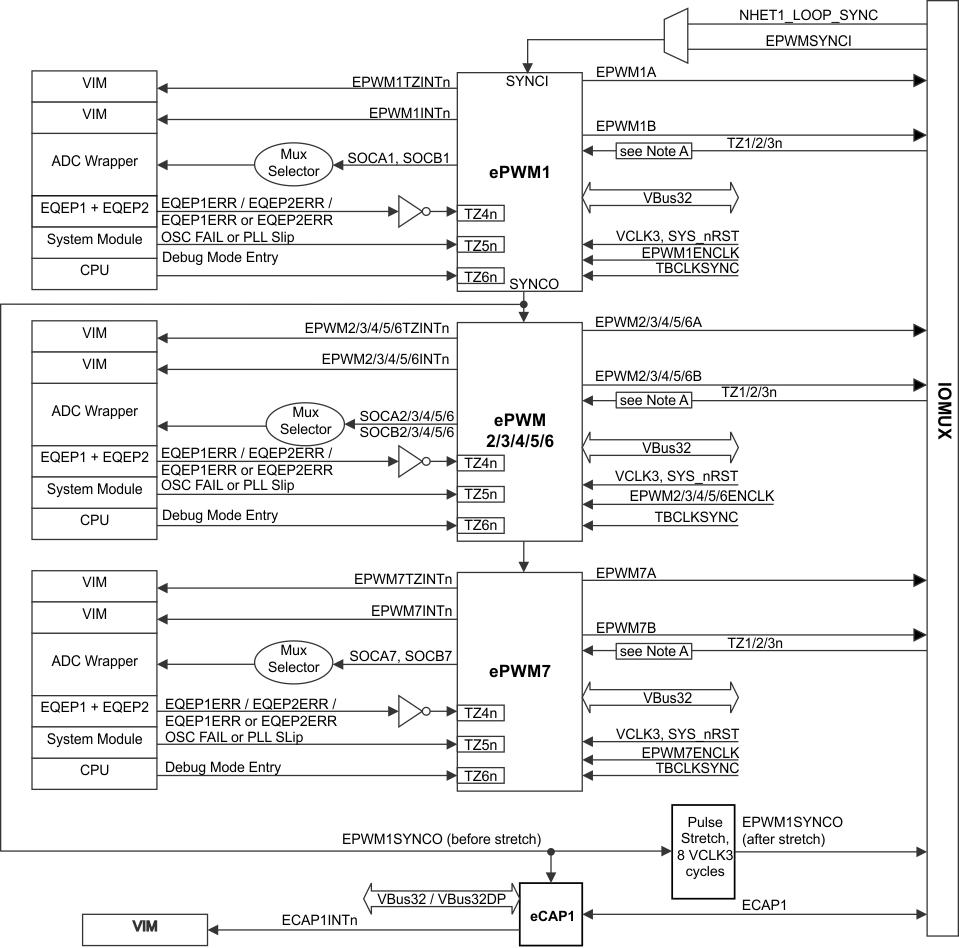
Figure 7-2 shows the detailed input synchronization selection (asynchronous, double-synchronous, or double synchronous + filter width) for ePWMx.
 Figure 7-2 ePWMx Input Synchronization Selection Detail
7.1.1 ePWM Clocking and Reset
Each ePWM module has a clock enable (ePWMxENCLK) which is controlled by its respective Peripheral Power Down bit in the PSPWRDWNCLRx register of the PCR2 module. To properly reset the peripherals, the peripherals must be released from reset by setting the PENA bit of the CLKCNTL register in the system module. In additional, the peripherals must be released from their power down state by clearing their respective bit in the PSPWRDWNCLRx register. By default after reset, the peripherals are in powerdown state.
Table 7-1 ePWMx Clock Enable Control
| ePWM MODULE INSTANCE | CONTROL REGISTER TO ENABLE CLOCK |
DEFAULT VALUE |
|---|---|---|
| ePWM1 | PSPWRDWNCLR3[16] | 1 |
| ePWM2 | PSPWRDWNCLR3[17] | 1 |
| ePWM3 | PSPWRDWNCLR3[18] | 1 |
| ePWM4 | PSPWRDWNCLR3[19] | 1 |
| ePWM5 | PSPWRDWNCLR3[12] | 1 |
| ePWM6 | PSPWRDWNCLR3[13] | 1 |
| ePWM7 | PSPWRDWNCLR3[14] | 1 |
7.1.2 Synchronization of ePWMx Time-Base Counters
A time-base synchronization scheme connects all of the ePWM modules on a device. Each ePWM module has a synchronization input (EPWMxSYNCI) and a synchronization output (EPWMxSYNCO). The input synchronization for the first instance (ePWM1) comes from an external pin. Figure 7-1 shows the synchronization connections for all the ePWMx modules. Each ePWM module can be configured to use or ignore the synchronization input. For more information, see the ePWM module chapter of the device-specific TRM.
7.1.3 Synchronizing all ePWM Modules to the N2HET1 Module Time Base
The connection between the NHET1_LOOP_SYNC and the SYNCI input of ePWM1 module is implemented as shown in Figure 7-3.
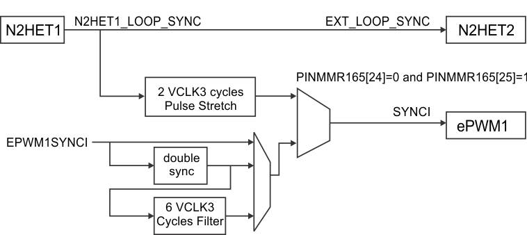 Figure 7-3 Synchronizing Time Bases Between N2HET1, N2HET2 and ePWMx Modules
7.1.4 Phase-Locking the Time-Base Clocks of Multiple ePWM Modules
The TBCLKSYNC bit can be used to globally synchronize the time-base clocks of all enabled ePWM modules on a device. This bit is implemented as PINMMR166[1] register bit 1.
When TBCLKSYNC = 0, the time-base clock of all ePWM modules is stopped. This is the default condition.
When TBCLKSYNC = 1, all ePWM time-base clocks are started with the rising edge of TBCLK aligned.
For perfectly synchronized TBCLKs, the prescaler bits in the TBCTL register of each ePWM module must be set identically. The proper procedure for enabling the ePWM clocks is as follows:
- Each ePWM is individually associated with a power down bit in the PSPWRDWNCLRx register of the PCR2 module. Enable the individual ePWM module clocks (if disable) using the control registers in the PCR2.
- Configure TBCLKSYNC = 0. This will stop the time-base clock within any enabled ePWM module.
- Configure the prescaler values and desired ePWM modes.
- Configure TBCLKSYNC = 1.
7.1.5 ePWM Synchronization with External Devices
The output sync from the ePWM1 module is also exported to the I/O Mux such that multiple devices can be synchronized together. The signal pulse must be stretched by 8 VCLK3 cycles before being exported on the IO Mux pin as the ePWMSYNCO signal.
7.1.6 ePWM Trip Zones
The ePWMx modules have 6 trip zone inputs each. These are active-low signals. The application can control the ePWMx module response to each of the trip zone input separately. The timing requirements from the assertion of the trip zone inputs to the actual response are specified in the electrical and timing section of this document.
7.1.6.1 Trip Zones TZ1n, TZ2n, TZ3n
These 3 trip zone inputs are driven by external circuits and are connected to device-level inputs. These signals are either connected asynchronously to the ePWMx trip zone inputs, or double-synchronized with VCLK3, or double-synchronized and then filtered with a 6-cycle VCLK3-based counter before connecting to the ePWMx (see Figure 7-2). By default, the trip zone inputs are asynchronously connected to the ePWMx modules.
Table 7-2 Connection to ePWMx Modules for Device-Level Trip Zone Inputs
| TRIP ZONE INPUT |
CONTROL FOR ASYNCHRONOUS CONNECTION TO ePWMx |
CONTROL FOR DOUBLE-SYNCHRONIZED CONNECTION TO ePWMx |
CONTROL FOR DOUBLE-SYNCHRONIZED AND FILTERED CONNECTION TO ePWMx(1) |
|---|---|---|---|
| TZ1n | PINMMR172[18:16] = 001 | PINMMR172[18:16] = 010 | PINMMR172[18:16] = 100 |
| TZ2n | PINMMR172[26:24] = 001 | PINMMR172[26:24] = 010 | PINMMR172[26:24] = 100 |
| TZ3n | PINMMR173[2:0] = 001 | PINMMR173[2:0] = 010 | PINMMR173[2:0] = 100 |
7.1.6.2 Trip Zone TZ4n
This trip zone input is dedicated to eQEPx error indications. There are 2 eQEP modules on this device. Each eQEP module indicates a phase error by driving its EQEPxERR output high. The following control registers allow the application to configure the trip zone input (TZ4n) to each ePWMx module based on the requirements of the applicationapplication's requirements.
Table 7-3 TZ4n Connections for ePWMx Modules
| ePWMx | CONTROL FOR TZ4n = NOT(EQEP1ERR OR EQEP2ERR) |
CONTROL FOR TZ4n = NOT(EQEP1ERR) |
CONTROL FOR TZ4n = NOT(EQEP2ERR) |
|---|---|---|---|
| ePWM1 | PINMMR167[2:0] = 001 | PINMMR167[2:0] = 010 | PINMMR167[2:0] = 100 |
| ePWM2 | PINMMR167[10:8] = 001 | PINMMR167[10:8] = 010 | PINMMR167[10:8] = 100 |
| ePWM3 | PINMMR167[18:16] = 001 | PINMMR167[18:16] = 010 | PINMMR167[18:16] = 100 |
| ePWM4 | PINMMR167[26:24] = 001 | PINMMR167[26:24] = 010 | PINMMR167[26:24] = 100 |
| ePWM5 | PINMMR168[2:0] = 001 | PINMMR168[2:0] = 010 | PINMMR168[2:0] = 100 |
| ePWM6 | PINMMR168[10:8] = 001 | PINMMR168[10:8] = 010 | PINMMR168[10:8] = 100 |
| ePWM7 | PINMMR168[18:16] = 001 | PINMMR168[18:16] = 010 | PINMMR168[18:16] = 100 |
NOTE
The EQEPxERR signal is an active high signal coming out of EQEPx module. As listed in Table 7-3, the selected combination of the EQEPxERR signals must be inverted before connecting to the TZ4n input of the ePWMx modules.
7.1.6.3 Trip Zone TZ5n
This trip zone input is dedicated to a clock failure on the device. That is, this trip zone input is asserted whenever an oscillator failure or a PLL slip is detected on the device. The applciation can use this trip zone input for each ePWMx module to prevent the external system from going out of control when the device clocks are not within expected range (system running at limp clock).
The oscillator failure and PLL slip signals used for this trip zone input are taken from the status flags in the system module. These level signals are set until cleared by the application.
7.1.6.4 Trip Zone TZ6n
This trip zone input to the ePWMx modules is dedicated to a debug mode entry of the CPU. If enabled, the user can force the PWM outputs to a known state when the emulator stops the CPU. This prevents the external system from going out of control when the CPU is stopped.
NOTE
There is a signal called DBGACK that the CPU drives when it enters debug mode. This signal must be inverted and used as the Debug Mode Entry signal for the trip zone input.
7.1.7 Triggering of ADC Start of Conversion Using ePWMx SOCA and SOCB Outputs
A special scheme is implemented to select the actual signal used for triggering the start of conversion on the two ADCs on this device. This scheme is defined in Section 7.4.2.3.
7.1.8 Enhanced Translator-Pulse Width Modulator (ePWMx) Electrical Data/Timing
Table 7-4 ePWMx Timing Requirements
| TEST CONDITIONS | MIN | MAX | UNIT | ||
|---|---|---|---|---|---|
| tw(SYNCIN) | Synchronization input pulse width | Asynchronous | 2 tc(VCLK3) | cycles | |
| Synchronous | 2 tc(VCLK3) | cycles | |||
| Synchronous with input filter | 2 tc(VCLK3) + filter width(1) | cycles | |||
Table 7-5 ePWMx Switching Characteristics
| PARAMETER | TEST CONDITIONS | MIN | MAX | UNIT | |
|---|---|---|---|---|---|
| tw(PWM) | Pulse duration, ePWMx output high or low | 33.33 | ns | ||
| tw(SYNCOUT) | Synchronization Output Pulse Width | 8 tc(VCLK3) | cycles | ||
| td(PWM)tza | Delay time, trip input active to PWM forced high, OR Delay time, trip input active to PWM forced low | No pin load | 25 | ns | |
| td(TZ-PWM)HZ | Delay time, trip input active to PWM Hi-Z | 20 | ns | ||
Table 7-6 ePWMx Trip-Zone Timing Requirements
| TEST CONDITIONS | MIN | MAX | UNIT | ||
|---|---|---|---|---|---|
| tw(TZ) | Pulse duration, TZn input low | Asynchronous | 2 * TBePWMx | cycles | |
| Synchronous | 2 tc(VCLK3) | ||||
| Synchronous with input filter | 2 tc(VCLK3) + filter width(1) | ||||
7.2 Enhanced Capture Modules (eCAP)
Figure 7-4 shows how the eCAP modules are interconnected on this microcontroller.
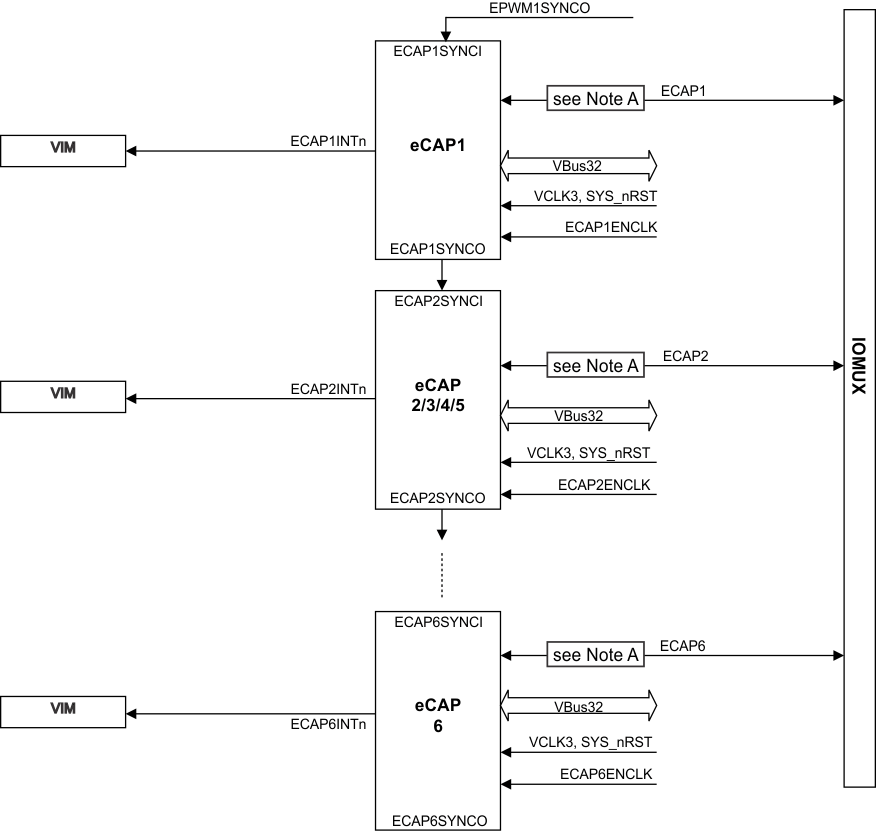
Figure 7-5 shows the detailed input synchronization selection (asynchronous, double-synchronous, or double synchronous + filter width) for eCAPx.
 Figure 7-5 eCAPx Input Synchronization Selection Detail
7.2.1 Clock Enable Control for eCAPx Modules
Each of the eCAPx modules has a clock enable (ECAPxENCLK) which is controlled by its respective Peripheral Power Down bit in the PSPWRDWNCLRx register of the PCR2 module. To properly reset the peripherals, the peripherals must be released from reset by setting the PENA bit of the CLKCNTL register in the system module. In addition, the peripherals must be released from their power down state by clearing the respective bit in the PSPWRDWNCLRx register. By default, after reset, the peripherals are in the power down state.
7.2.2 PWM Output Capability of eCAPx
When not used in capture mode, each of the eCAPx modules can be used as a single-channel PWM output. This is called the Auxiliary PWM (APWM) mode of operation of the eCAPx modules. For more information, see the eCAP module chapter of the device-specific TRM.
7.2.3 Input Connection to eCAPx Modules
The input connection to each of the eCAPx modules can be selected between a double-VCLK3-synchronized input or a double-VCLK3-synchronized and filtered input, as listed in Table 7-8.
Table 7-8 Device-Level Input Connection to eCAPx Modules
| INPUT SIGNAL | CONTROL FOR DOUBLE-SYNCHRONIZED CONNECTION TO eCAPx |
CONTROL FOR DOUBLE-SYNCHRONIZED AND FILTERED CONNECTION TO eCAPx(1) |
|---|---|---|
| eCAP1 | PINMMR169[2:0] = 001 | PINMMR169[2:0] = 010 |
| eCAP2 | PINMMR169[10:8] = 001 | PINMMR169[10:8] = 010 |
| eCAP3 | PINMMR169[18:16] = 001 | PINMMR169[18:16] = 010 |
| eCAP4 | PINMMR169[26:24] = 001 | PINMMR169[26:24] = 010 |
| eCAP5 | PINMMR170[2:0] = 001 | PINMMR170[2:0] = 010 |
| eCAP6 | PINMMR170[10:8] = 001 | PINMMR170[10:8] = 010 |
7.2.4 Enhanced Capture Module (eCAP) Electrical Data/Timing
Table 7-9 eCAPx Timing Requirements
| TEST CONDITIONS | MIN | MAX | UNIT | ||
|---|---|---|---|---|---|
| tw(CAP) | Pulse width, capture input | Synchronous | 2 tc(VCLK3) | cycles | |
| Synchronous with input filter | 2 tc(VCLK3) + filter width(1) | cycles | |||
Table 7-10 eCAPx Switching Characteristics
| PARAMETER | TEST CONDITIONS | MIN | MAX | UNIT | |
|---|---|---|---|---|---|
| tw(APWM) | Pulse duration, APWMx output high or low | 20 | ns | ||
7.3 Enhanced Quadrature Encoder (eQEP)
Figure 7-6 shows the eQEP module interconnections on the device.
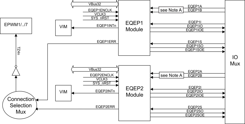
Figure 7-7 shows the detailed input synchronization selection (asynchronous, double-synchronous, or double synchronous + filter width) for eQEPx.
 Figure 7-7 eQEPx Input Synchronization Selection Detail
7.3.1 Clock Enable Control for eQEPx Modules
Each of the EQEPx modules has a clock enable (EQEPxENCLK) which is controlled by its respective Peripheral Power Down bit in the PSPWRDWNCLRx register of the PCR2 module. To properly reset the peripherals, the peripherals must be released from reset by setting the PENA bit of the CLKCNTL register in the system module. In addition, the peripherals must be released from their power down state by clearing the respective bit in the PSPWRDWNCLRx register. By default after reset, the peripherals are in power down state.
7.3.2 Using eQEPx Phase Error to Trip ePWMx Outputs
The eQEP module sets the EQEPERR signal output whenever a phase error is detected in its inputs EQEPxA and EQEPxB. This error signal from both the eQEP modules is input to the connection selection multiplexer. This multiplexer is defined in Table 7-3. As shown in Figure 7-6, the output of this selection multiplexer is inverted and connected to the TZ4n trip-zone input of all ePWMx modules. This connection allows the application to define the response of each ePWMx module on a phase error indicated by the eQEP modules.
7.3.3 Input Connection to eQEPx Modules
The input connection to each of the eQEP modules can be selected between a double-VCLK3-synchronized input or a double-VCLK3-synchronized and filtered input, as listed in Table 7-12.
Table 7-12 Device-Level Input Connection to eQEPx Modules
| INPUT SIGNAL | CONTROL FOR DOUBLE-SYNCHRONIZED CONNECTION TO eQEPx |
CONTROL FOR DOUBLE-SYNCHRONIZED AND FILTERED CONNECTION(1) TO eQEPx |
|---|---|---|
| eQEP1A | PINMMR170[18:16] = 001 | PINMMR170[18:16] = 010 |
| eQEP1B | PINMMR170[26:24] = 001 | PINMMR170[26:24] = 010 |
| eQEP1I | PINMMR171[2:0] = 001 | PINMMR171[2:0] = 010 |
| eQEP1S | PINMMR171[10:8] = 001 | PINMMR171[10:8] = 010 |
| eQEP2A | PINMMR171[18:16] = 001 | PINMMR171[18:16] = 010 |
| eQEP2B | PINMMR171[26:24] = 001 | PINMMR171[26:24] = 010 |
| eQEP2I | PINMMR172[2:0] = 001 | PINMMR172[2:0] = 010 |
| eQEP2S | PINMMR172[10:8] = 001 | PINMMR172[10:8] = 010 |
7.3.4 Enhanced Quadrature Encoder Pulse (eQEPx) Timing
Table 7-13 eQEPx Timing Requirements(1)
| TEST CONDITIONS | MIN | MAX | UNIT | ||
|---|---|---|---|---|---|
| tw(QEPP) | QEP input period | Synchronous | 2 tc(VCLK3) | cycles | |
| Synchronous with input filter | 2 tc(VCLK3) + filter width | ||||
| tw(INDEXH) | QEP Index Input High Time | Synchronous | 2 tc(VCLK3) | cycles | |
| Synchronous with input filter | 2 tc(VCLK3) + filter width | ||||
| tw(INDEXL) | QEP Index Input Low Time | Synchronous | 2 tc(VCLK3) | cycles | |
| Synchronous with input filter | 2 tc(VCLK3) + filter width | ||||
| tw(STROBH) | QEP Strobe Input High Time | Synchronous | 2 tc(VCLK3) | cycles | |
| Synchronous with input filter | 2 tc(VCLK3) + filter width | ||||
| tw(STROBL) | QEP Strobe Input Low Time | Synchronous | 2 tc(VCLK3) | cycles | |
| Synchronous with input filter | 2 tc(VCLK3) + filter width | ||||
Table 7-14 eQEPx Switching Characteristics
| PARAMETER | MIN | MAX | UNIT | |
|---|---|---|---|---|
| td(CNTR)xin | Delay time, external clock to counter increment | 4 tc(VCLK3) | cycles | |
| td(PCS-OUT)QEP | Delay time, QEP input edge to position compare sync output | 6 tc(VCLK3) | cycles | |
7.4 12-bit Multibuffered Analog-to-Digital Converter (MibADC)
The MibADC has a separate power bus for its analog circuitry that enhances the Analog-to-Digital (A-to-D) performance by preventing digital switching noise on the logic circuitry which could be present on VSS and VCC from coupling into the A-to-D analog stage. All A-to-D specifications are given with respect to ADREFLO, unless otherwise noted.
Table 7-15 MibADC Overview
| DESCRIPTION | VALUE |
|---|---|
| Resolution | 12 bits |
| Monotonic | Assured |
| Output conversion code | 00h to FFFh [00 for VAI ≤ ADREFLO; FFF for VAI ≥ ADREFHI] |
7.4.1 MibADC Features
- 10-/12-bit resolution
- ADREFHI and ADREFLO pins (high and low reference voltages)
- Total Sample/Hold/Convert time: 600 ns Typical Minimum at 30 MHz ADCLK
- One memory region per conversion group is available (Event Group, Group 1, and Group 2)
- Allocation of channels to conversion groups is completely programmable
- Memory regions are serviced either by interrupt or by DMA
- Programmable interrupt threshold counter is available for each group
- Programmable magnitude threshold interrupt for each group for any one channel
- Option to read either 8-, 10-, or 12-bit values from memory regions
- Single or continuous conversion modes
- Embedded self-test
- Embedded calibration logic
- Enhanced power-down mode
- Optional feature to automatically power down ADC core when no conversion is in progress
- External event pin (ADEVT) programmable as general-purpose I/O
7.4.2 Event Trigger Options
The ADC module supports three conversion groups: Event Group, Group1, and Group2. Each of these three groups can be configured to be triggered by a hardware event. In that case, the application can select from among eight event sources to be the trigger for a group's conversions.
7.4.2.1 MibADC1 Event Trigger Hookup
Table 7-16 lists the event sources that can trigger the conversions for the MibADC1 groups.
Table 7-16 MibADC1 Event Trigger Selection
| GROUP SOURCE SELECT BITS (G1SRC, G2SRC OR EVSRC) |
EVENT NO. | PINMMR161[0] | PINMMR161[1] | CONTROL FOR OPTION A |
CONTROL FOR OPTION B |
TRIGGER SOURCE |
|---|---|---|---|---|---|---|
| 000 | 1 | x | x | — | — | AD1EVT |
| 001 | 2 | 1 | 0 | PINMMR161[8] = x | PINMMR161[9] = x | N2HET1[8] |
| 0 | 1 | PINMMR161[8] = 1 | PINMMR161[9] = 0 | N2HET2[5] | ||
| 0 | 1 | PINMMR161[8] = 0 | PINMMR161[9] = 1 | e_TPWM_B | ||
| 010 | 3 | 1 | 0 | — | — | N2HET1[10] |
| 0 | 1 | — | — | N2HET1[27] | ||
| 011 | 4 | 1 | 0 | PINMMR161[16] = x | PINMMR161[17] = x | RTI1 Comp0 |
| 0 | 1 | PINMMR161[16] = 1 | PINMMR161[17] = 0 | RTI1 Comp0 | ||
| 0 | 1 | PINMMR161[16] = 0 | PINMMR161[17] = 1 | e_TPWM_A1 | ||
| 100 | 5 | 1 | 0 | — | — | N2HET1[12] |
| 0 | 1 | — | — | N2HET1[17] | ||
| 101 | 6 | 1 | 0 | PINMMR161[24] = x | PINMMR161[25] = x | N2HET1[14] |
| 0 | 1 | PINMMR161[24] = 1 | PINMMR161[25] = 0 | N2HET1[19] | ||
| 0 | 1 | PINMMR161[24] = 0 | PINMMR161[25] = 1 | N2HET2[1] | ||
| 110 | 7 | 1 | 0 | PINMMR162[0] = x | PINMMR162[1] = x | GIOB[0] |
| 0 | 1 | PINMMR162[0] = 1 | PINMMR162[1] = 0 | N2HET1[11] | ||
| 0 | 1 | PINMMR162[0] = 0 | PINMMR162[1] = 1 | ePWM_A2 | ||
| 111 | 8 | 1 | 0 | PINMMR162[8] = x | PINMMR162[9] = x | GIOB[1] |
| 0 | 1 | PINMMR162[8] = 1 | PINMMR162[9] = 0 | N2HET2[13] | ||
| 0 | 1 | PINMMR162[8] = 0 | PINMMR162[9] = 1 | ePWM_AB |
NOTE
For ADEVT trigger source, the connection to the MibADC1 module trigger input is made from the output side of the input buffer. This way, a trigger condition can be generated either by configuring ADEVT as an output function on to the pad (through the mux control), or by driving the ADEVT signal from an external trigger source as input. If the mux control module is used to select different functionality instead of the ADEVT signal, then care must be taken to disable ADEVT from triggering conversions; there is no multiplexing on the input connection.
If ePWM_B, ePWM_A2, ePWM_AB, N2HET2[1], N2HET2[5], N2HET2[13], N2HET1[11], N2HET1[17], or N2HET1[19] is used to trigger the ADC, the connection to the ADC is made directly from the N2HET or ePWM module outputs. As a result, the ADC can be triggered without having to enable the signal from being output on a device terminal.
NOTE
For N2HETx trigger sources, the connection to the MibADC1 module trigger input is made from the input side of the output buffer (at the N2HETx module boundary). This way, a trigger condition can be generated even if the N2HETx signal is not selected to be output on the pad.
NOTE
For the RTI compare 0 interrupt source, the connection is made directly from the output of the RTI module. That is, the interrupt condition can be used as a trigger source even if the actual interrupt is not signaled to the CPU.
7.4.2.2 MibADC2 Event Trigger Hookup
Table 7-17 lists the event sources that can trigger the conversions for the MibADC2 groups.
Table 7-17 MibADC2 Event Trigger Selection
| GROUP SOURCE SELECT BITS (G1SRC, G2SRC, or EVSRC) |
EVENT NO. | PINMMR161[0] | PINMMR161[1] | CONTROL FOR OPTION A |
CONTROL FOR OPTION B |
TRIGGER SOURCE |
|---|---|---|---|---|---|---|
| 000 | 1 | x | x | NA | NA | AD2EVT |
| 001 | 2 | 1 | 0 | PINMMR162[16] = x | PINMMR162[17] = x | N2HET1[8] |
| 0 | 1 | PINMMR162[16] = 1 | PINMMR162[17] = 0 | N2HET2[5] | ||
| 0 | 1 | PINMMR162[16] = 0 | PINMMR162[17] = 1 | e_TPWM_B | ||
| 010 | 3 | 1 | 0 | NA | NA | N2HET1[10] |
| 0 | 1 | NA | NA | N2HET1[27] | ||
| 011 | 4 | 1 | 0 | PINMMR162[24] = x | PINMMR162[25] = x | RTI1 Comp0 |
| 0 | 1 | PINMMR162[24] = 1 | PINMMR162[25] = 0 | RTI1 Comp0 | ||
| 0 | 1 | PINMMR162[24] = 0 | PINMMR162[25] = 1 | e_TPWM_A1 | ||
| 100 | 5 | 1 | 0 | NA | NA | N2HET1[12] |
| 0 | 1 | NA | NA | N2HET1[17] | ||
| 101 | 6 | 1 | 0 | PINMMR163[0] = x | PINMMR163[0] = x | N2HET1[14] |
| 0 | 1 | PINMMR163[0] = 1 | PINMMR163[0] = 0 | N2HET1[19] | ||
| 0 | 1 | PINMMR163[0] = 0 | PINMMR163[0] = 1 | N2HET2[1] | ||
| 110 | 7 | 1 | 0 | PINMMR163[8] = x | PINMMR163[8] = x | GIOB[0] |
| 0 | 1 | PINMMR163[8] = 1 | PINMMR163[8] = 0 | N2HET1[11] | ||
| 0 | 1 | PINMMR163[8] = 0 | PINMMR163[8] = 1 | ePWM_A2 | ||
| 111 | 8 | 1 | 0 | PINMMR163[16] = x | PINMMR163[16] = x | GIOB[1] |
| 0 | 1 | PINMMR163[16] = 1 | PINMMR163[16] = 0 | N2HET2[13] | ||
| 0 | 1 | PINMMR163[16] = 0 | PINMMR163[16] = 1 | ePWM_AB |
NOTE
For AD2EVT trigger source, the connection to the MibADC2 module trigger input is made from the output side of the input buffer. This way, a trigger condition can be generated either by configuring AD2EVT as an output function on to the pad (through the mux control), or by driving the AD2EVT signal from an external trigger source as input. If the mux control module is used to select different functionality instead of the AD2EVT signal, then care must be taken to disable AD2EVT from triggering conversions; there is no multiplexing on the input connections.
If ePWM_B, ePWM_A2, ePWM_AB, N2HET2[1], N2HET2[5], N2HET2[13], N2HET1[11], N2HET1[17], or N2HET1[19] is used to trigger the ADC, the connection to the ADC is made directly from the N2HET or ePWM module outputs. As a result, the ADC can be triggered without having to enable the signal from being output on a device terminal.
NOTE
For N2HETx trigger sources, the connection to the MibADC2 module trigger input is made from the input side of the output buffer (at the N2HETx module boundary). This way, a trigger condition can be generated even if the N2HETx signal is not selected to be output on the pad.
NOTE
For the RTI compare 0 interrupt source, the connection is made directly from the output of the RTI module. That is, the interrupt condition can be used as a trigger source even if the actual interrupt is not signaled to the CPU.
7.4.2.3 Controlling ADC1 and ADC2 Event Trigger Options Using SOC Output from ePWM Modules
As shown in Figure 7-8, the ePWMxSOCA and ePWMxSOCB outputs from each ePWM module are used to generate four signals – ePWM_B, ePWM_A1, ePWM_A2, and ePWM_AB, that are available to trigger the ADC based on the application requirement.
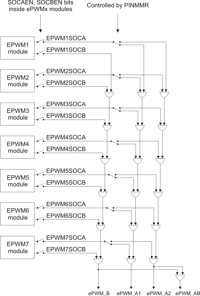 Figure 7-8 ADC Trigger Source Generation from ePWMx
Table 7-18 Control Bit to SOC Output
| CONTROL BIT | SOC OUTPUT |
|---|---|
| PINMMR164[0] | SOC1A_SEL |
| PINMMR164[8] | SOC2A_SEL |
| PINMMR164[16] | SOC3A_SEL |
| PINMMR164[24] | SOC4A_SEL |
| PINMMR165[0] | SOC5A_SEL |
| PINMMR165[8] | SOC6A_SEL |
| PINMMR165[16] | SOC7A_SEL |
The SOCA output from each ePWM module is connected to a "switch" shown in Figure 7-8. This switch is implemented by using the control registers in the PINMMR module. Figure 7-9 is an example of the implementation is shown for the switch on SOC1A. The switches on the other SOCA signals are implemented in the same way.
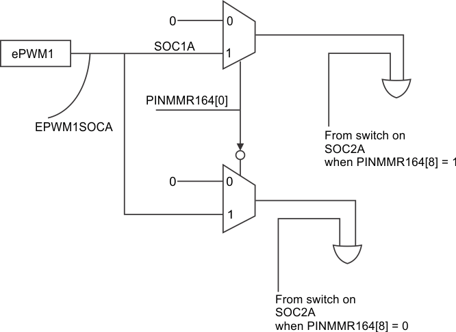 Figure 7-9 ePWM1SOC1A Switch Implementation
The logic equations for the four outputs from the combinational logic shown in Figure 7-8 are:
| ePWM_B = | SOC1B or SOC2B or SOC3B or SOC4B or SOC5B or SOC6B or SOC7B | (1) |
| ePWM_A1 = | [ SOC1A and not(SOC1A_SEL) ] or [ SOC2A and not(SOC2A_SEL) ] or [ SOC3A and not(SOC3A_SEL) ] or | (2) |
| [ SOC4A and not(SOC4A_SEL) ] or [ SOC5A and not(SOC5A_SEL) ] or [ SOC6A and not(SOC6A_SEL) ] or | ||
| [ SOC7A and not(SOC7A_SEL) ] | ||
| ePWM_A2 = | [ SOC1A and SOC1A_SEL ] or [ SOC2A and SOC2A_SEL ] or [ SOC3A and SOC3A_SEL ] or | (3) |
| [ SOC4A and SOC4A_SEL ] or [ SOC5A and SOC5A_SEL ] or [ SOC6A and SOC6A_SEL ] or | ||
| [ SOC7A and SOC7A_SEL ] | ||
| ePWM_AB = | ePWM_B or ePWM_A2 | (4) |
7.4.3 ADC Electrical and Timing Specifications
Table 7-19 MibADC Recommended Operating Conditions
| PARAMETER | MIN | MAX | UNIT | |
|---|---|---|---|---|
| ADREFHI | A-to-D high-voltage reference source | ADREFLO | VCCAD(1) | V |
| ADREFLO | A-to-D low-voltage reference source | VSSAD(1) | ADREFHI | V |
| VAI | Analog input voltage | ADREFLO | ADREFHI | V |
| IAIC | Analog input clamp current(2) (VAI < VSSAD – 0.3 or VAI > VCCAD + 0.3) | –2 | 2 | mA |
Table 7-20 MibADC Electrical Characteristics Over Full Ranges of Recommended Operating Conditions(2)
| PARAMETER | DESCRIPTION/CONDITIONS | MIN | MAX | UNIT | ||
|---|---|---|---|---|---|---|
| Rmux | Analog input mux on-resistance | See Figure 7-10 | 250 | Ω | ||
| Rsamp | ADC sample switch on-resistance | See Figure 7-10 | 250 | Ω | ||
| Cmux | Input mux capacitance | See Figure 7-10 | 16 | pF | ||
| Csamp | ADC sample capacitance | See Figure 7-10 | 13 | pF | ||
| IAIL | Analog off-state input leakage current | VCCAD = 3.6 V | VSSAD ≤ VIN < VSSAD + 100 mV | –300 | 200 | nA |
| VSSAD + 100 mV ≤ VIN ≤ VCCAD - 200 mV | –200 | 200 | ||||
| VCCAD - 200 mV < VIN ≤ VCCAD | –200 | 500 | ||||
| IAIL | Analog off-state input leakage current | VCCAD = 5.25 V | VSSAD ≤ VIN < VSSAD + 300 mV | –1000 | 250 | nA |
| VSSAD + 300 mV ≤ VIN ≤ VCCAD - 300 mV | –250 | 250 | ||||
| VCCAD - 300 mV < VIN ≤ VCCAD | –250 | 1000 | ||||
| IAOSB(1) | Analog on-state input bias current | VCCAD = 3.6 V | VSSAD ≤ VIN < VSSAD + 100 mV | –10 | 2 | µA |
| VSSAD + 100 mV < VIN < VCCAD - 200 mV | –4 | 2 | ||||
| VCCAD - 200 mV < VIN < VCCAD | –4 | 16 | ||||
| IAOSB(1) | Analog on-state input bias current | VCCAD = 5.25 V | VSSAD ≤ VIN < VSSAD + 300 mV | –12 | 3 | µA |
| VSSAD + 300 mV ≤ VIN ≤ VCCAD - 300 mV | –5 | 3 | ||||
| VCCAD - 300 mV < VIN ≤ VCCAD | –5 | 18 | ||||
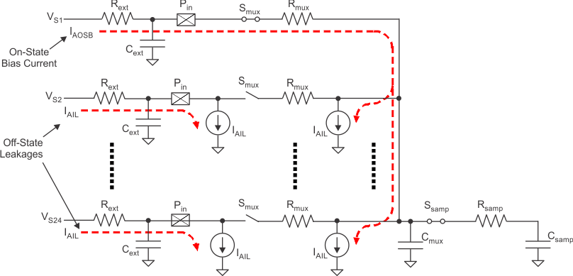 Figure 7-10 MibADC Input Equivalent Circuit
Table 7-21 MibADC Timing Specifications
| PARAMETER | MIN | NOM | MAX | UNIT | |
|---|---|---|---|---|---|
| tc(ADCLK)(1) | Cycle time, MibADC clock | 0.033 | µs | ||
| td(SH)(2) | Delay time, sample and hold time | 0.2 | µs | ||
| 12-BIT MODE | |||||
| td(C) | Delay time, conversion time | 0.4 | µs | ||
| td(SHC)(3) | Delay time, total sample/hold and conversion time | 0.6 | µs | ||
| 10-BIT MODE | |||||
| td(C) | Delay time, conversion time | 0.33 | µs | ||
| td(SHC)(3) | Delay time, total sample/hold and conversion time | 0.53 | µs | ||
Table 7-22 MibADC Operating Characteristics Over 3.0 V to 3.6 V Operating Conditions(1)(2)
| PARAMETER | DESCRIPTION/CONDITIONS | MIN | MAX | UNIT | ||
|---|---|---|---|---|---|---|
| CR | Conversion range over which specified accuracy is maintained | ADREFHI - ADREFLO | 3 | 3.6 | V | |
| ZSET | Zero Scale Offset | Difference between the first ideal transition (from code 000h to 001h) and the actual transition | 10-bit mode | 1 | LSB | |
| 12-bit mode | 2 | LSB | ||||
| FSET | Full Scale Offset | Difference between the range of the measured code transitions (from first to last) and the range of the ideal code transitions | 10-bit mode | 2 | LSB | |
| 12-bit mode | 3 | LSB | ||||
| EDNL | Differential nonlinearity error | Difference between the actual step width and the ideal value. (See Figure 7-11) | 10-bit mode | –1 | 1.5 | LSB |
| 12-bit mode | –1 | 2 | LSB | |||
| EINL | Integral nonlinearity error | Maximum deviation from the best straight line through the MibADC. MibADC transfer characteristics, excluding the quantization error. | 10-bit mode | –2 | 2 | LSB |
| 12-bit mode | –2 | 2 | LSB | |||
| ETOT | Total unadjusted error (after calibration) | Maximum value of the difference between an analog value and the ideal midstep value. | 10-bit mode | –2 | 2 | LSB |
| 12-bit mode | –4 | 4 | LSB | |||
Table 7-23 MibADC Operating Characteristics Over 3.6 V to 5.25 V Operating Conditions(1)(2)
| PARAMETER | DESCRIPTION/CONDITIONS | MIN | MAX | UNIT | ||
|---|---|---|---|---|---|---|
| CR | Conversion range over which specified accuracy is maintained | ADREFHI - ADREFLO | 3.6 | 5.25 | V | |
| ZSET | Zero Scale Offset | Difference between the first ideal transition (from code 000h to 001h) and the actual transition | 10-bit mode | 1 | LSB | |
| 12-bit mode | 2 | LSB | ||||
| FSET | Full Scale Offset | Difference between the range of the measured code transitions (from first to last) and the range of the ideal code transitions | 10-bit mode | 2 | LSB | |
| 12-bit mode | 3 | LSB | ||||
| EDNL | Differential nonlinearity error | Difference between the actual step width and the ideal value. (See Figure 7-11) | 10-bit mode | –1 | 1.5 | LSB |
| 12-bit mode | –1 | 3 | LSB | |||
| EINL | Integral nonlinearity error | Maximum deviation from the best straight line through the MibADC. MibADC transfer characteristics, excluding the quantization error. | 10-bit mode | –2 | 2 | LSB |
| 12-bit mode | –4.5 | 2 | LSB | |||
| ETOT | Total unadjusted error (after calibration) | Maximum value of the difference between an analog value and the ideal midstep value. | 10-bit mode | –2 | 2 | LSB |
| 12-bit mode | –6 | 5 | LSB | |||
7.4.4 Performance (Accuracy) Specifications
7.4.4.1 MibADC Nonlinearity Errors
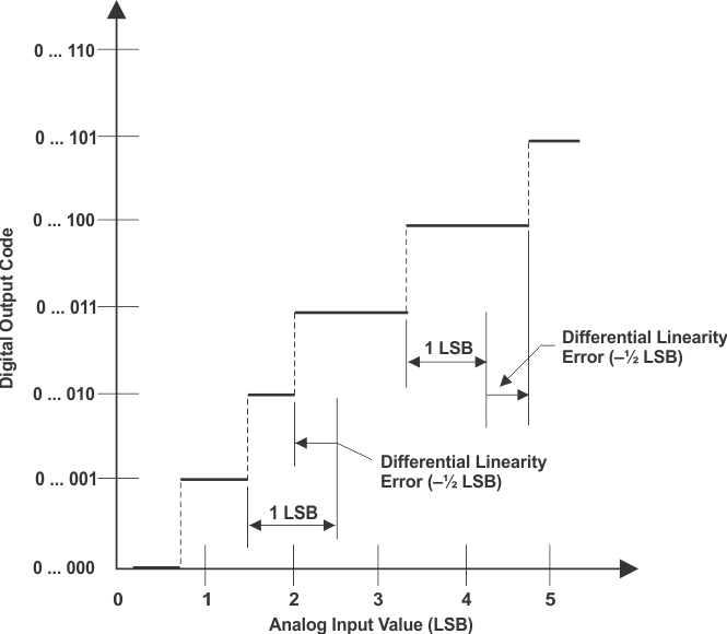
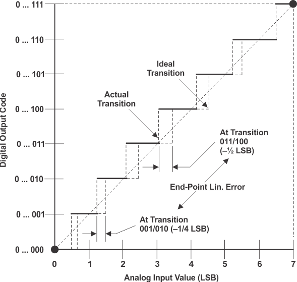
The differential nonlinearity error shown in Figure 7-11 (sometimes referred to as differential linearity) is the difference between an actual step width and the ideal value of 1 LSB.
The integral nonlinearity error shown in Figure 7-12 (sometimes referred to as linearity error) is the deviation of the values on the actual transfer function from a straight line.
7.4.4.2 MibADC Total Error
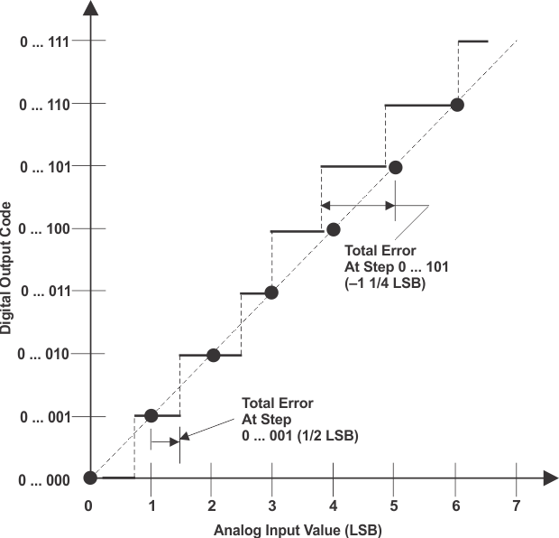
The absolute accuracy or total error of an MibADC as shown in Figure 7-13 is the maximum value of the difference between an analog value and the ideal midstep value.
7.5 General-Purpose Input/Output
The GPIO module on this device supports two ports, GIOA and GIOB. The I/O pins are bidirectional and bit-programmable. Both GIOA and GIOB support external interrupt capability.
7.5.1 Features
The GPIO module has the following features:
- Each I/O pin can be configured as:
- Input
- Output
- Open Drain
- The interrupts have the following characteristics:
- Programmable interrupt detection either on both edges or on a single edge (set in GIOINTDET)
- Programmable edge-detection polarity, either rising or falling edge (set in GIOPOL register)
- Individual interrupt flags (set in GIOFLG register)
- Individual interrupt enables, set and cleared through GIOENASET and GIOENACLR registers respectively
- Programmable interrupt priority, set through GIOLVLSET and GIOLVLCLR registers
- Internal pullup/pulldown allows unused I/O pins to be left unconnected
For information on input and output timings see Section 5.10.1 and Section 5.10.2.
7.6 Enhanced High-End Timer (N2HET)
The N2HET is an advanced intelligent timer that provides sophisticated timing functions for real-time applications. The timer is software-controlled, using a reduced instruction set, with a specialized timer micromachine and an attached I/O port. The N2HET can be used for pulse width modulated outputs, capture or compare inputs, or general-purpose I/O.. It is especially well suited for applications requiring multiple sensor information and drive actuators with complex and accurate time pulses.
7.6.1 Features
The N2HET module has the following features:
- Programmable timer for input and output timing functions
- Reduced instruction set (30 instructions) for dedicated time and angle functions
- 256 words of instruction RAM protected by parity
- User defined number of 25-bit virtual counters for timer, event counters and angle counters
- 7-bit hardware counters for each pin allow up to 32-bit resolution in conjunction with the 25-bit virtual counters
- Up to 32 pins usable for input signal measurements or output signal generation
- Programmable suppression filter for each input pin with adjustable limiting frequency
- Low CPU overhead and interrupt load
- Efficient data transfer to or from the CPU memory with dedicated High-End-Timer Transfer Unit (HTU) or DMA
- Diagnostic capabilities with different loopback mechanisms and pin status readback functionality
7.6.2 N2HET RAM Organization
The timer RAM uses 4 RAM banks, where each bank has two port access capability. This means that one RAM address may be written while another address is read. The RAM words are 96-bits wide, which are split into three 32-bit fields (program, control, and data).
7.6.3 Input Timing Specifications
The N2HET instructions PCNT and WCAP impose some timing constraints on the input signals.
 Figure 7-14 N2HET Input Capture Timings
Table 7-24 Dynamic Characteristics for the N2HET Input Capture Functionality
| PARAMETER | MIN | MAX | UNIT | |
|---|---|---|---|---|
| 1 | Input signal period, PCNT or WCAP for rising edge to rising edge | (HRP) (LRP) tc(VCLK2) + 2 | 225 (HRP) (LRP) tc(VCLK2) - 2 | ns |
| 2 | Input signal period, PCNT or WCAP for falling edge to falling edge | (HRP) (LRP) tc(VCLK2) + 2 | 225 (HRP) (LRP) tc(VCLK2) - 2 | ns |
| 3 | Input signal high phase, PCNT or WCAP for rising edge to falling edge | 2 (HRP) tc(VCLK2) + 2 | 225 (HRP) (LRP) tc(VCLK2) - 2 | ns |
| 4 | Input signal low phase, PCNT or WCAP for falling edge to rising edge | 2 (HRP) tc(VCLK2) + 2 | 225 (HRP) (LRP) tc(VCLK2) - 2 | ns |
7.6.4 N2HET1-N2HET2 Interconnections
In some applications the N2HET resolutions must be synchronized. Some other applications require a single time base to be used for all PWM outputs and input timing captures.
The N2HET provides such a synchronization mechanism. The Clk_master/slave (HETGCR.16) configures the N2HET in master or slave mode (default is slave mode). A N2HET in master mode provides a signal to synchronize the prescalers of the slave N2HET. The slave N2HET synchronizes its loop resolution to the loop resolution signal sent by the master. The slave does not require this signal after it receives the first synchronization signal. However, anytime the slave receives the resynchronization signal from the master, the slave must synchronize itself again..
 Figure 7-15 N2HET1 – N2HET2 Synchronization Hookup
7.6.5 N2HET Checking
7.6.5.1 Internal Monitoring
To assure correctness of the high-end timer operation and output signals, the two N2HET modules can be used to monitor each other’s signals as shown in Figure 7-16. The direction of the monitoring is controlled by the I/O multiplexing control module.
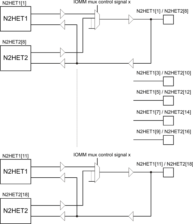 Figure 7-16 N2HET Monitoring
7.6.5.2 Output Monitoring using Dual Clock Comparator (DCC)
N2HET1[31] is connected as a clock source for counter 1 in DCC1. This allows the application to measure the frequency of the pulse-width modulated (PWM) signal on N2HET1[31].
Similarly, N2HET2[0] is connected as a clock source for counter 1 in DCC2. This allows the application to measure the frequency of the pulse-width modulated (PWM) signal on N2HET2[0].
Both N2HET1[31] and N2HET2[0] can be configured to be internal-only channels. That is, the connection to the DCC module is made directly from the output of the N2HETx module (from the input of the output buffer).
For more information on DCC see Section 6.7.3.
7.6.6 Disabling N2HET Outputs
Some applications require the N2HET outputs to be disabled under some fault condition. The N2HET module provides this capability through the "Pin Disable" input signal. This signal, when driven low, causes the N2HET outputs identified by a programmable register (HETPINDIS) to be tri-stated. Refer to the IOMM chapter in the device specific technical reference manual for more details on the "N2HET Pin Disable" feature.
GIOA[5] is connected to the "Pin Disable" input for N2HET1, and GIOB[2] is connected to the "Pin Disable" input for N2HET2.
7.6.7 High-End Timer Transfer Unit (HET-TU)
A High End Timer Transfer Unit (HET-TU) can perform DMA type transactions to transfer N2HET data to or from main memory. A Memory Protection Unit (MPU) is built into the HET-TU.
7.6.7.1 Features
- CPU and DMA independent
- Master Port to access system memory
- 8 control packets supporting dual buffer configuration
- Control packet information is stored in RAM protected by parity
- Event synchronization (HET transfer requests)
- Supports 32 or 64 bit transactions
- Addressing modes for HET address (8 byte or 16 byte) and system memory address (fixed, 32 bit or 64bit)
- One shot, circular and auto switch buffer transfer modes
- Request lost detection
7.6.7.2 Trigger Connections
Table 7-25 HET TU1 Request Line Connection
| Modules | Request Source | HET TU1 Request |
|---|---|---|
| N2HET1 | HTUREQ[0] | HET TU1 DCP[0] |
| N2HET1 | HTUREQ[1] | HET TU1 DCP[1] |
| N2HET1 | HTUREQ[2] | HET TU1 DCP[2] |
| N2HET1 | HTUREQ[3] | HET TU1 DCP[3] |
| N2HET1 | HTUREQ[4] | HET TU1 DCP[4] |
| N2HET1 | HTUREQ[5] | HET TU1 DCP[5] |
| N2HET1 | HTUREQ[6] | HET TU1 DCP[6] |
| N2HET1 | HTUREQ[7] | HET TU1 DCP[7] |
Table 7-26 HET TU2 Request Line Connection
| Modules | Request Source | HET TU2 Request |
|---|---|---|
| N2HET2 | HTUREQ[0] | HET TU2 DCP[0] |
| N2HET2 | HTUREQ[1] | HET TU2 DCP[1] |
| N2HET2 | HTUREQ[2] | HET TU2 DCP[2] |
| N2HET2 | HTUREQ[3] | HET TU2 DCP[3] |
| N2HET2 | HTUREQ[4] | HET TU2 DCP[4] |
| N2HET2 | HTUREQ[5] | HET TU2 DCP[5] |
| N2HET2 | HTUREQ[6] | HET TU2 DCP[6] |
| N2HET2 | HTUREQ[7] | HET TU2 DCP[7] |
7.7 FlexRay Interface
The FlexRay module performs communication according to the FlexRay protocol specification v2.1. The sample clock bitrate can be programmed to values up to 10 MBit per second. Additional bus driver (BD) hardware is required for connection to the physical layer.
For communication on a FlexRay network, individual message buffers with up to 254 data bytes are configurable. The message storage consists of a single-ported message RAM that holds up to 128 message buffers. All functions concerning the handling of messages are implemented in the message handler. Those functions are the acceptance filtering, the transfer of messages between the two FlexRay Channel Protocol Controllers and the message RAM, maintaining the transmission schedule as well as providing message status information.
The register set of the FlexRay module can be accessed directly by the CPU through the VBUS interface. These registers are used to control, configure and monitor the FlexRay channel protocol controllers, message handler, global time unit, system universal control, frame/symbol processing, network management, interrupt control, and to access the message RAM through the I/O buffer.
7.7.1 Features
The FlexRay module has the following features:
- Conformance with FlexRay protocol specification v2.1
- Data rates of up to 10 Mbps on each channel
- Up to 128 message buffers
- 8KB of message RAM for storage of for example, 128 message buffers with max. 48 byte data section or up to 30 message buffers with 254 byte data section
- Configuration of message buffers with different payload lengths
- One configurable receive FIFO
- Each message buffer can be configured as receive buffer, as transmit buffer or as part of the receive FIFO
- CPU access to message buffers through input and output buffer
- FlexRay Transfer Unit (FTU) for automatic data transfer between data memory and message buffers without CPU interaction
- Filtering for slot counter, cycle counter, and channel ID
- Maskable module interrupts
- Supports Network Management
- ECC protection on the message RAM
7.7.2 Electrical and Timing Specifications
Table 7-27 Timing Requirements for FlexRay Inputs(1)
| Parameter | MIN | MAX | UNIT | |
|---|---|---|---|---|
| tpw | Input minimum pulse width to meet the FlexRay sampling requirement | tc(VCLKA2) + 2.5(2) | ns | |
 Figure 7-17 FlexRay Inputs
Table 7-28 FlexRay Jitter Timing(2)
| PARAMETER | MIN | MAX | UNIT | |
|---|---|---|---|---|
| tTx1bit | Clock jitter and signal symmetry | 98 | 102 | ns |
| tTx10bit | FlexRay BSS (byte start sequence) to BSS | 999 | 1001 | ns |
| tTx10bitAvg | Average over 10000 samples | 999.5 | 1000.5 | ns |
| tRxAsymDelay(1) | Delay difference between rise and fall from Rx pin to sample point in FlexRay core | – | 2.5 | ns |
| tjit(SCLK) | Jitter for the 80-MHz Sample Clock generated by the PLL | – | 0.5 | ns |
7.7.3 FlexRay Transfer Unit
The FlexRay Transfer Unit is able to transfer data between the input buffer (IBF) and output buffer (OBF) of the communication controller and the system memory without CPU interaction.
Because the FlexRay module is accessed through the FTU, the FTU must be powered up by the setting bit 23 in the Peripheral Power Down Registers of the System Module before accessing any FlexRay module register.
For more information on the FTU see the device specific technical reference manual.
7.8 Controller Area Network (DCAN)
The DCAN supports the CAN 2.0B protocol standard and uses a serial, multimaster communication protocol that efficiently supports distributed real-time control with robust communication rates of up to 1 megabit per second (Mbps). The DCAN is ideal for applications operating in noisy and harsh environments (e.g., automotive and industrial fields) that require reliable serial communication or multiplexed wiring.
7.8.1 Features
Features of the DCAN module include:
- Supports CAN protocol version 2.0 part A, B
- Bit rates up to 1 MBit/s
- The CAN kernel can be clocked by the oscillator for baud-rate generation.
- 64 mailboxes on each DCAN
- Individual identifier mask for each message object
- Programmable FIFO mode for message objects
- Programmable loop-back modes for self-test operation
- Automatic bus on after Bus-Off state by a programmable 32-bit timer
- Message RAM protected by ECC
- Direct access to Message RAM during test mode
- CAN Rx / Tx pins configurable as general purpose IO pins
- Message RAM Auto Initialization
- DMA support
For more information on the DCAN see the device specific technical reference manual.
7.8.2 Electrical and Timing Specifications
Table 7-29 Dynamic Characteristics for the DCANx TX and RX pins
| Parameter | MIN | MAX | Unit | |
|---|---|---|---|---|
| td(CANnTX) | Delay time, transmit shift register to CANnTX pin(1) | 15 | ns | |
| td(CANnRX) | Delay time, CANnRX pin to receive shift register | 5 | ns | |
7.9 Local Interconnect Network Interface (LIN)
The SCI/LIN module can be programmed to work either as an SCI or as a LIN. The core of the module is an SCI. The SCI’s hardware features are augmented to achieve LIN compatibility.
The SCI module is a universal asynchronous receiver-transmitter that implements the standard nonreturn to zero format. The SCI can be used to communicate, for example, through an RS-232 port or over a K-line.
The LIN standard is based on the SCI (UART) serial data link format. The communication concept is single-master/multiple-slave with a message identification for multicast transmission between any network nodes.
7.9.1 LIN Features
The following are features of the LIN module:
- Compatible to LIN 1.3, 2.0 and 2.1 protocols
- Multibuffered receive and transmit units DMA capability for minimal CPU intervention
- Identification masks for message filtering
- Automatic Master Header Generation
- Programmable Synch Break Field
- Synch Field
- Identifier Field
- Slave Automatic Synchronization
- Synch break detection
- Optional baudrate update
- Synchronization Validation
- 231 programmable transmission rates with 7 fractional bits
- Error detection
- 2 Interrupt lines with priority encoding
7.10 Serial Communication Interface (SCI)
7.10.1 Features
- Standard universal asynchronous receiver-transmitter (UART) communication
- Supports full- or half-duplex operation
- Standard nonreturn to zero (NRZ) format
- Double-buffered receive and transmit functions
- Configurable frame format of 3 to 13 bits per character based on the following:
- Data word length programmable from one to eight bits
- Additional address bit in address-bit mode
- Parity programmable for zero or one parity bit, odd or even parity
- Stop programmable for one or two stop bits
- Asynchronous or isosynchronous communication modes
- Two multiprocessor communication formats allow communication between more than two devices.
- Sleep mode is available to free CPU resources during multiprocessor communication.
- The 24-bit programmable baud rate supports 224 different baud rates provide high accuracy baud rate selection.
- Four error flags and Five status flags provide detailed information regarding SCI events.
- Capability to use DMA for transmit and receive data.
7.11 Inter-Integrated Circuit (I2C)
The inter-integrated circuit (I2C) module is a multimaster communication module providing an interface between the TMS570 microcontroller and devices compliant with Philips Semiconductor I2C-bus specification version 2.1 and connected by an I2C-bus. This module will support any slave or master I2C compatible device.
7.11.1 Features
The I2C has the following features:
- Compliance to the Philips I2C bus specification, v2.1 (The I2C Specification, Philips document number 9398 393 40011)
- Bit/Byte format transfer
- 7-bit and 10-bit device addressing modes
- General call
- START byte
- Multimaster transmitter/ slave receiver mode
- Multimaster receiver/ slave transmitter mode
- Combined master transmit/receive and receive/transmit mode
- Transfer rates of 10 kbps up to 400 kbps (Phillips fast-mode rate)
- Free data format
- Two DMA events (transmit and receive)
- DMA event enable/disable capability
- Seven interrupts that can be used by the CPU
- Module enable/disable capability
- The SDA and SCL are optionally configurable as general purpose I/O
- Slew rate control of the outputs
- Open drain control of the outputs
- Programmable pullup/pulldown capability on the inputs
- Supports Ignore NACK mode
NOTE
This I2C module does not support:
- High-speed (HS) mode
- C-bus compatibility mode
- The combined format in 10-bit address mode (the I2C sends the slave address second byte every time it sends the slave address first byte)
7.11.2 I2C I/O Timing Specifications
Table 7-30 I2C Signals (SDA and SCL) Switching Characteristics(1)
| PARAMETER | STANDARD MODE | FAST MODE | UNIT | |||
|---|---|---|---|---|---|---|
| MIN | MAX | MIN | MAX | |||
| tc(I2CCLK) | Cycle time, Internal Module clock for I2C, prescaled from VCLK | 75.2 | 149 | 75.2 | 149 | ns |
| f(SCL) | SCL Clock frequency | 0 | 100 | 0 | 400 | kHz |
| tc(SCL) | Cycle time, SCL | 10 | 2.5 | µs | ||
| tsu(SCLH-SDAL) | Setup time, SCL high before SDA low (for a repeated START condition) | 4.7 | 0.6 | µs | ||
| th(SCLL-SDAL) | Hold time, SCL low after SDA low (for a repeated START condition) | 4 | 0.6 | µs | ||
| tw(SCLL) | Pulse duration, SCL low | 4.7 | 1.3 | µs | ||
| tw(SCLH) | Pulse duration, SCL high | 4 | 0.6 | µs | ||
| tsu(SDA-SCLH) | Setup time, SDA valid before SCL high | 250 | 100 | ns | ||
| th(SDA-SCLL) | Hold time, SDA valid after SCL low (for I2C bus devices) | 0 | 3.45(2) | 0 | 0.9 | µs |
| tw(SDAH) | Pulse duration, SDA high between STOP and START conditions | 4.7 | 1.3 | µs | ||
| tsu(SCLH-SDAH) | Setup time, SCL high before SDA high (for STOP condition) | 4.0 | 0.6 | µs | ||
| tw(SP) | Pulse duration, spike (must be suppressed) | 0 | 50 | ns | ||
| Cb(3) | Capacitive load for each bus line | 400 | 400 | pF | ||
 Figure 7-18 I2C Timings
NOTE
- A device must internally provide a hold time of at least 300 ns for the SDA signal (referred to the VIHmin of the SCL signal) to bridge the undefined region of the falling edge of SCL.
- The maximum th(SDA-SCLL) has only to be met if the device does not stretch the LOW period (tw(SCLL)) of the SCL signal.
- A Fast-mode I2C-bus device can be used in a Standard-mode I2C-bus system, but the requirement tsu(SDA-SCLH) ≥ 250 ns must then be met. This will automatically be the case if the device does not stretch the LOW period of the SCL signal. If such a device does stretch the LOW period of the SCL signal, it must output the next data bit to the SDA line tr max + tsu(SDA-SCLH).
- Cb = total capacitance of one bus line in pF. If mixed with fast-mode devices, faster fall-times are allowed.
7.12 Multibuffered / Standard Serial Peripheral Interface
The MibSPI is a high-speed synchronous serial input/output port that allows a serial bit stream of programmed length (2 to 16 bits) to be shifted in and out of the device at a programmed bit-transfer rate. Typical applications for the SPI include interfacing to external peripherals, such as I/Os, memories, display drivers, and analog-to-digital converters.
7.12.1 Features
Both Standard and MibSPI modules have the following features:
- 16-bit shift register
- Receive buffer register
- 11-bit baud clock generator
- SPICLK can be internally-generated (master mode) or received from an external clock source (slave mode)
- Each word transferred can have a unique format
- SPI I/Os not used in the communication can be used as digital input/output signals
Table 7-31 MibSPI Configurations
| MibSPIx/SPIx | I/Os |
|---|---|
| MibSPI1 | MIBSPI1SIMO[1:0], MIBSPI1SOMI[1:0], MIBSPI1CLK, MIBSPI1nCS[5:0], MIBSPI1nENA |
| MibSPI3 | MIBSPI3SIMO, MIBSPI3SOMI, MIBSPI3CLK, MIBSPI3nCS[5:0], MIBSPI3nENA |
| MibSPI5 | MIBSPI5SIMO[3:0], MIBSPI5SOMI[3:0], MIBSPI5CLK, MIBSPI5nCS[5:0], MIBSPI5nENA |
| MibSPI2 | MIBSPI2SIMO,MIBSPI2SOMI,MIBSPI2CLK,MIBSPI2nCS[1:0],MIBSPI2nENA |
| MibSPI4 | MIBSPI4SIMO,MIBSPI4SOMI,MIBSPI4CLK,MIBSPI4nCS[5:0],MIBSPI4nENA |
7.12.2 MibSPI Transmit and Receive RAM Organization
The Multibuffer RAM is comprised of 256 buffers for MibSPI1 and 128 buffers for all other MibSPI. Each entry in the Multibuffer RAM consists of 4 parts: a 16-bit transmit field, a 16-bit receive field, a 16-bit control field and a 16-bit status field. The Multibuffer RAM can be partitioned into multiple transfer groups with a variable number of buffers each.
7.12.3 MibSPI Transmit Trigger Events
Each of the transfer groups can be configured individually. For each of the transfer groups a trigger event and a trigger source can be chosen. A trigger event can be for example a rising edge or a permanent low level at a selectable trigger source. For example, up to 15 trigger sources are available which can be used by each transfer group.
7.12.3.1 MIBSPI1 Event Trigger Hookup
Table 7-32 MIBSPI1 Event Trigger Hookup
| Event # | TGxCTRL TRIGSRC[3:0] | Trigger |
|---|---|---|
| Disabled | 0000 | No trigger source |
| EVENT0 | 0001 | GIOA[0] |
| EVENT1 | 0010 | GIOA[1] |
| EVENT2 | 0011 | GIOA[2] |
| EVENT3 | 0100 | GIOA[3] |
| EVENT4 | 0101 | GIOA[4] |
| EVENT5 | 0110 | GIOA[5] |
| EVENT6 | 0111 | GIOA[6] |
| EVENT7 | 1000 | GIOA[7] |
| EVENT8 | 1001 | N2HET1[8] |
| EVENT9 | 1010 | N2HET1[10] |
| EVENT10 | 1011 | N2HET1[12] |
| EVENT11 | 1100 | N2HET1[14] |
| EVENT12 | 1101 | N2HET1[16] |
| EVENT13 | 1110 | N2HET1[18] |
| EVENT14 | 1111 | Intern Tick counter |
NOTE
For N2HET1 trigger sources, the connection to the MibSPI1 module trigger input is made from the input side of the output buffer (at the N2HET1 module boundary). This way, a trigger condition can be generated even if the N2HET1 signal is not selected to be output on the pad.
NOTE
For GIOx trigger sources, the connection to the MibSPI1 module trigger input is made from the output side of the input buffer. This way, a trigger condition can be generated either by selecting the GIOx pin as an output pin plus selecting the pin to be a GIOx pin, or by driving the GIOx pin from an external trigger source. If the mux control module is used to select different functionality instead of the GIOx signal, then care must be taken to disable GIOx from triggering MibSPI1 transfers; there is no multiplexing on the input connections.
7.12.3.2 MIBSPI2 Event Trigger Hookup
Table 7-33 MIBSPI2 Event Trigger Hookup
| Event # | TGxCTRL TRIGSRC[3:0] | Trigger |
|---|---|---|
| Disabled | 0000 | No trigger source |
| EVENT0 | 0001 | GIOA[0] |
| EVENT1 | 0010 | GIOA[1] |
| EVENT2 | 0011 | GIOA[2] |
| EVENT3 | 0100 | GIOA[3] |
| EVENT4 | 0101 | GIOA[4] |
| EVENT5 | 0110 | GIOA[5] |
| EVENT6 | 0111 | GIOA[6] |
| EVENT7 | 1000 | GIOA[7] |
| EVENT8 | 1001 | N2HET1[8] |
| EVENT9 | 1010 | N2HET1[10] |
| EVENT10 | 1011 | N2HET1[12] |
| EVENT11 | 1100 | N2HET1[14] |
| EVENT12 | 1101 | N2HET1[16] |
| EVENT13 | 1110 | N2HET1[18] |
| EVENT14 | 1111 | Intern Tick counter |
NOTE
For N2HET1 trigger sources, the connection to the MibSPI1 module trigger input is made from the input side of the output buffer (at the N2HET1 module boundary). This way, a trigger condition can be generated even if the N2HET1 signal is not selected to be output on the pad.
NOTE
For GIOx trigger sources, the connection to the MibSPI1 module trigger input is made from the output side of the input buffer. This way, a trigger condition can be generated either by selecting the GIOx pin as an output pin plus selecting the pin to be a GIOx pin, or by driving the GIOx pin from an external trigger source. If the mux control module is used to select different functionality instead of the GIOx signal, then care must be taken to disable GIOx from triggering MibSPI1 transfers; there is no multiplexing on the input connections.
7.12.3.3 MIBSPI3 Event Trigger Hookup
Table 7-34 MIBSPI3 Event Trigger Hookup
| Event # | TGxCTRL TRIGSRC[3:0] | Trigger |
|---|---|---|
| Disabled | 0000 | No trigger source |
| EVENT0 | 0001 | GIOA[0] |
| EVENT1 | 0010 | GIOA[1] |
| EVENT2 | 0011 | GIOA[2] |
| EVENT3 | 0100 | GIOA[3] |
| EVENT4 | 0101 | GIOA[4] |
| EVENT5 | 0110 | GIOA[5] |
| EVENT6 | 0111 | GIOA[6] |
| EVENT7 | 1000 | GIOA[7] |
| EVENT8 | 1001 | H2ET1[8] |
| EVENT9 | 1010 | N2HET1[10] |
| EVENT10 | 1011 | N2HET1[12] |
| EVENT11 | 1100 | N2HET1[14] |
| EVENT12 | 1101 | N2HET1[16] |
| EVENT13 | 1110 | N2HET1[18] |
| EVENT14 | 1111 | Intern Tick counter |
NOTE
For N2HET1 trigger sources, the connection to the MibSPI3 module trigger input is made from the input side of the output buffer (at the N2HET1 module boundary). This way, a trigger condition can be generated even if the N2HET1 signal is not selected to be output on the pad.
NOTE
For GIOx trigger sources, the connection to the MibSPI3 module trigger input is made from the output side of the input buffer. This way, a trigger condition can be generated either by selecting the GIOx pin as an output pin plus selecting the pin to be a GIOx pin, or by driving the GIOx pin from an external trigger source. If the mux control module is used to select different functionality instead of the GIOx signal, then care must be taken to disable GIOx from triggering MibSPI3 transfers; there is no multiplexing on the input connections.
7.12.3.4 MIBSPI4 Event Trigger Hookup
Table 7-35 MIBSPI4 Event Trigger Hookup
| Event # | TGxCTRL TRIGSRC[3:0] | Trigger |
|---|---|---|
| Disabled | 0000 | No trigger source |
| EVENT0 | 0001 | GIOA[0] |
| EVENT1 | 0010 | GIOA[1] |
| EVENT2 | 0011 | GIOA[2] |
| EVENT3 | 0100 | GIOA[3] |
| EVENT4 | 0101 | GIOA[4] |
| EVENT5 | 0110 | GIOA[5] |
| EVENT6 | 0111 | GIOA[6] |
| EVENT7 | 1000 | GIOA[7] |
| EVENT8 | 1001 | N2HET1[8] |
| EVENT9 | 1010 | N2HET1[10] |
| EVENT10 | 1011 | N2HET1[12] |
| EVENT11 | 1100 | N2HET1[14] |
| EVENT12 | 1101 | N2HET1[16] |
| EVENT13 | 1110 | N2HET1[18] |
| EVENT14 | 1111 | Intern Tick counter |
NOTE
For N2HET1 trigger sources, the connection to the MibSPI1 module trigger input is made from the input side of the output buffer (at the N2HET1 module boundary). This way, a trigger condition can be generated even if the N2HET1 signal is not selected to be output on the pad.
NOTE
For GIOx trigger sources, the connection to the MibSPI1 module trigger input is made from the output side of the input buffer. This way, a trigger condition can be generated either by selecting the GIOx pin as an output pin plus selecting the pin to be a GIOx pin, or by driving the GIOx pin from an external trigger source. If the mux control module is used to select different functionality instead of the GIOx signal, then care must be taken to disable GIOx from triggering MibSPI1 transfers; there is no multiplexing on the input connections.
7.12.3.5 MIBSPI5 Event Trigger Hookup
Table 7-36 MIBSPI5 Event Trigger Hookup
| Event # | TGxCTRL TRIGSRC[3:0] | Trigger |
| Disabled | 0000 | No trigger source |
| EVENT0 | 0001 | GIOA[0] |
| EVENT1 | 0010 | GIOA[1] |
| EVENT2 | 0011 | GIOA[2] |
| EVENT3 | 0100 | GIOA[3] |
| EVENT4 | 0101 | GIOA[4] |
| EVENT5 | 0110 | GIOA[5] |
| EVENT6 | 0111 | GIOA[6] |
| EVENT7 | 1000 | GIOA[7] |
| EVENT8 | 1001 | N2HET1[8] |
| EVENT9 | 1010 | N2HET1[10] |
| EVENT10 | 1011 | N2HET1[12] |
| EVENT11 | 1100 | N2HET1[14] |
| EVENT12 | 1101 | N2HET1[16] |
| EVENT13 | 1110 | N2HET1[18] |
| EVENT14 | 1111 | Intern Tick counter |
NOTE
For N2HET1 trigger sources, the connection to the MibSPI5 module trigger input is made from the input side of the output buffer (at the N2HET1 module boundary). This way, a trigger condition can be generated even if the N2HET1 signal is not selected to be output on the pad.
NOTE
For GIOx trigger sources, the connection to the MibSPI5 module trigger input is made from the output side of the input buffer. This way, a trigger condition can be generated either by selecting the GIOx pin as an output pin + selecting the pin to be a GIOx pin, or by driving the GIOx pin from an external trigger source. If the mux control module is used to select different functionality instead of the GIOx signal, then care must be taken to disable GIOx from triggering MibSPI5 transfers; there is no multiplexing on the input connections.
7.12.4 MibSPI/SPI Master Mode I/O Timing Specifications
Table 7-37 SPI Master Mode External Timing Parameters (CLOCK PHASE = 0, SPICLK = output, SPISIMO = output, and SPISOMI = input)(1)(2)(3)
| NO. | Parameter | MIN | MAX | Unit | ||
|---|---|---|---|---|---|---|
| 1 | tc(SPC)M | Cycle time, SPICLK(4) | 40 | 256tc(VCLK) | ns | |
| 2(5) | tw(SPCH)M | Pulse duration, SPICLK high (clock polarity = 0) | 0.5tc(SPC)M – tr(SPC)M – 3 | 0.5tc(SPC)M + 3 | ns | |
| tw(SPCL)M | Pulse duration, SPICLK low (clock polarity = 1) | 0.5tc(SPC)M – tf(SPC)M – 3 | 0.5tc(SPC)M + 3 | |||
| 3(5) | tw(SPCL)M | Pulse duration, SPICLK low (clock polarity = 0) | 0.5tc(SPC)M – tf(SPC)M – 3 | 0.5tc(SPC)M + 3 | ns | |
| tw(SPCH)M | Pulse duration, SPICLK high (clock polarity = 1) | 0.5tc(SPC)M – tr(SPC)M – 3 | 0.5tc(SPC)M + 3 | |||
| 4(5) | td(SPCH-SIMO)M | Delay time, SPISIMO valid before SPICLK low (clock polarity = 0) | 0.5tc(SPC)M – 6 | ns | ||
| td(SPCL-SIMO)M | Delay time, SPISIMO valid before SPICLK high (clock polarity = 1) | 0.5tc(SPC)M – 6 | ||||
| 5(5) | tv(SPCL-SIMO)M | Valid time, SPISIMO data valid after SPICLK low (clock polarity = 0) | 0.5tc(SPC)M – tf(SPC) – 4 | ns | ||
| tv(SPCH-SIMO)M | Valid time, SPISIMO data valid after SPICLK high (clock polarity = 1) | 0.5tc(SPC)M – tr(SPC) – 4 | ||||
| 6(5) | tsu(SOMI-SPCL)M | Setup time, SPISOMI before SPICLK low (clock polarity = 0) | tf(SPC) + 2.2 | ns | ||
| tsu(SOMI-SPCH)M | Setup time, SPISOMI before SPICLK high (clock polarity = 1) | tr(SPC) + 2.2 | ||||
| 7(5) | th(SPCL-SOMI)M | Hold time, SPISOMI data valid after SPICLK low (clock polarity = 0) | 10 | ns | ||
| th(SPCH-SOMI)M | Hold time, SPISOMI data valid after SPICLK high (clock polarity = 1) | 10 | ||||
| 8(6) | tC2TDELAY | Setup time CS active until SPICLK high (clock polarity = 0) | CSHOLD = 0 | C2TDELAY*tc(VCLK) + 2*tc(VCLK) - tf(SPICS) + tr(SPC) – 7 | (C2TDELAY+2) * tc(VCLK) - tf(SPICS) + tr(SPC) + 5.5 | ns |
| CSHOLD = 1 | C2TDELAY*tc(VCLK) + 3*tc(VCLK) - tf(SPICS) + tr(SPC) – 7 | (C2TDELAY+3) * tc(VCLK) - tf(SPICS) + tr(SPC) + 5.5 | ||||
| Setup time CS active until SPICLK low (clock polarity = 1) | CSHOLD = 0 | C2TDELAY*tc(VCLK) + 2*tc(VCLK) - tf(SPICS) + tf(SPC) – 7 | (C2TDELAY+2) * tc(VCLK) - tf(SPICS) + tf(SPC) + 5.5 | ns | ||
| CSHOLD = 1 | C2TDELAY*tc(VCLK) + 3*tc(VCLK) - tf(SPICS) + tf(SPC) – 7 | (C2TDELAY+3) * tc(VCLK) - tf(SPICS) + tf(SPC) + 5.5 | ||||
| 9(6) | tT2CDELAY | Hold time SPICLK low until CS inactive (clock polarity = 0) | 0.5*tc(SPC)M + T2CDELAY*tc(VCLK) + tc(VCLK) - tf(SPC) + tr(SPICS) - 7 | 0.5*tc(SPC)M + T2CDELAY*tc(VCLK) + tc(VCLK) - tf(SPC) + tr(SPICS) + 11 | ns | |
| Hold time SPICLK high until CS inactive (clock polarity = 1) | 0.5*tc(SPC)M + T2CDELAY*tc(VCLK) + tc(VCLK) - tr(SPC) + tr(SPICS) - 7 | 0.5*tc(SPC)M + T2CDELAY*tc(VCLK) + tc(VCLK) - tr(SPC) + tr(SPICS) + 11 | ns | |||
| 10 | tSPIENA | SPIENAn Sample point | (C2TDELAY+1) * tc(VCLK) - tf(SPICS) – 29 | (C2TDELAY+1)*tc(VCLK) | ns | |
| 11 | tSPIENAW | SPIENAn Sample point from write to buffer | (C2TDELAY+2)*tc(VCLK) | ns | ||
For PS values from 1 to 255: tc(SPC)M ≥ (PS +1)tc(VCLK) ≥ 40ns, where PS is the prescale value set in the SPIFMTx.[15:8] register bits.
For PS values of 0: tc(SPC)M = 2tc(VCLK) ≥ 40ns.
The external load on the SPICLK pin must be less than 60pF.
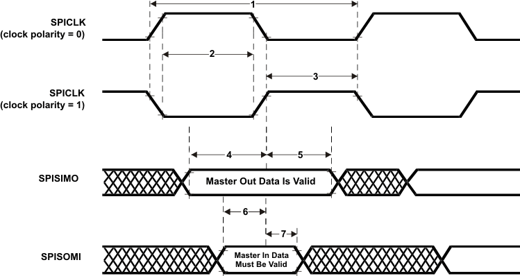 Figure 7-19 SPI Master Mode External Timing (CLOCK PHASE = 0)
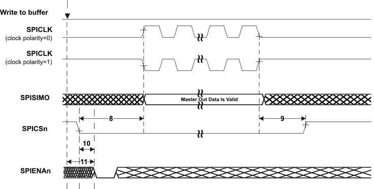 Figure 7-20 SPI Master Mode Chip Select Timing (CLOCK PHASE = 0)
Table 7-38 SPI Master Mode External Timing Parameters (CLOCK PHASE = 1, SPICLK = output, SPISIMO = output, and SPISOMI = input)(1)(2)(3)
| NO. | Parameter | MIN | MAX | Unit | ||
|---|---|---|---|---|---|---|
| 1 | tc(SPC)M | Cycle time, SPICLK (4) | 40 | 256tc(VCLK) | ns | |
| 2(5) | tw(SPCH)M | Pulse duration, SPICLK high (clock polarity = 0) | 0.5tc(SPC)M – tr(SPC)M – 3 | 0.5tc(SPC)M + 3 | ns | |
| tw(SPCL)M | Pulse duration, SPICLK low (clock polarity = 1) | 0.5tc(SPC)M – tf(SPC)M – 3 | 0.5tc(SPC)M + 3 | |||
| 3(5) | tw(SPCL)M | Pulse duration, SPICLK low (clock polarity = 0) | 0.5tc(SPC)M – tf(SPC)M – 3 | 0.5tc(SPC)M + 3 | ns | |
| tw(SPCH)M | Pulse duration, SPICLK high (clock polarity = 1) | 0.5tc(SPC)M – tr(SPC)M – 3 | 0.5tc(SPC)M + 3 | |||
| 4(5) | tv(SIMO-SPCH)M | Valid time, SPICLK high after SPISIMO data valid (clock polarity = 0) | 0.5tc(SPC)M – 6 | ns | ||
| tv(SIMO-SPCL)M | Valid time, SPICLK low after SPISIMO data valid (clock polarity = 1) | 0.5tc(SPC)M – 6 | ||||
| 5(5) | tv(SPCH-SIMO)M | Valid time, SPISIMO data valid after SPICLK high (clock polarity = 0) | 0.5tc(SPC)M – tr(SPC) – 4 | ns | ||
| tv(SPCL-SIMO)M | Valid time, SPISIMO data valid after SPICLK low (clock polarity = 1) | 0.5tc(SPC)M – tf(SPC) – 4 | ||||
| 6(5) | tsu(SOMI-SPCH)M | Setup time, SPISOMI before SPICLK high (clock polarity = 0) | tr(SPC) + 2.2 | ns | ||
| tsu(SOMI-SPCL)M | Setup time, SPISOMI before SPICLK low (clock polarity = 1) | tf(SPC) + 2.2 | ||||
| 7(5) | tv(SPCH-SOMI)M | Valid time, SPISOMI data valid after SPICLK high (clock polarity = 0) | 10 | ns | ||
| tv(SPCL-SOMI)M | Valid time, SPISOMI data valid after SPICLK low (clock polarity = 1) | 10 | ||||
| 8(6) | tC2TDELAY | Setup time CS active until SPICLK high (clock polarity = 0) | CSHOLD = 0 | 0.5*tc(SPC)M + (C2TDELAY+2) * tc(VCLK) - tf(SPICS) + tr(SPC) – 7 | 0.5*tc(SPC)M + (C2TDELAY+2) * tc(VCLK) - tf(SPICS) + tr(SPC) + 5.5 | ns |
| CSHOLD = 1 | 0.5*tc(SPC)M + (C2TDELAY+3) * tc(VCLK) - tf(SPICS) + tr(SPC) – 7 | 0.5*tc(SPC)M + (C2TDELAY+3) * tc(VCLK) - tf(SPICS) + tr(SPC) + 5.5 | ||||
| Setup time CS active until SPICLK low (clock polarity = 1) | CSHOLD = 0 | 0.5*tc(SPC)M + (C2TDELAY+2) * tc(VCLK) - tf(SPICS) + tf(SPC) – 7 | 0.5*tc(SPC)M + (C2TDELAY+2) * tc(VCLK) - tf(SPICS) + tf(SPC) + 5.5 | ns | ||
| CSHOLD = 1 | 0.5*tc(SPC)M + (C2TDELAY+3) * tc(VCLK) - tf(SPICS) + tf(SPC) – 7 | 0.5*tc(SPC)M + (C2TDELAY+3) * tc(VCLK) - tf(SPICS) + tf(SPC) + 5.5 | ||||
| 9(6) | tT2CDELAY | Hold time SPICLK low until CS inactive (clock polarity = 0) | T2CDELAY*tc(VCLK) + tc(VCLK) - tf(SPC) + tr(SPICS) - 7 | T2CDELAY*tc(VCLK) + tc(VCLK) - tf(SPC) + tr(SPICS) + 11 | ns | |
| Hold time SPICLK high until CS inactive (clock polarity = 1) | T2CDELAY*tc(VCLK) + tc(VCLK) - tr(SPC) + tr(SPICS) - 7 | T2CDELAY*tc(VCLK) + tc(VCLK) - tr(SPC) + tr(SPICS) + 11 | ns | |||
| 10 | tSPIENA | SPIENAn Sample Point | (C2TDELAY+1)* tc(VCLK) - tf(SPICS) – 29 | (C2TDELAY+1)*tc(VCLK) | ns | |
| 11 | tSPIENAW | SPIENAn Sample point from write to buffer | (C2TDELAY+2)*tc(VCLK) | ns | ||
For PS values from 1 to 255: tc(SPC)M ≥ (PS +1)tc(VCLK) ≥ 40ns, where PS is the prescale value set in the SPIFMTx.[15:8] register bits.
For PS values of 0: tc(SPC)M = 2tc(VCLK) ≥ 40ns.
The external load on the SPICLK pin must be less than 60pF.
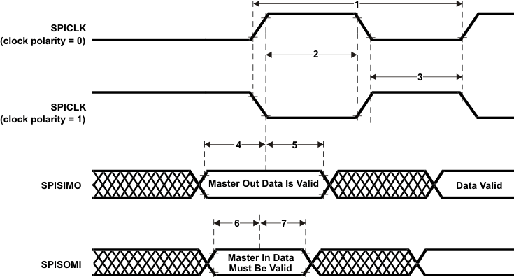 Figure 7-21 SPI Master Mode External Timing (CLOCK PHASE = 1)
 Figure 7-22 SPI Master Mode Chip Select Timing (CLOCK PHASE = 1)
7.12.5 SPI Slave Mode I/O Timings
Table 7-39 SPI Slave Mode External Timing Parameters (CLOCK PHASE = 0, SPICLK = input, SPISIMO = input, and SPISOMI = output)(1)(2)(3)(4)
| NO. | Parameter | MIN | MAX | Unit | |
|---|---|---|---|---|---|
| 1 | tc(SPC)S | Cycle time, SPICLK(5) | 40 | ns | |
| 2(6) | tw(SPCH)S | Pulse duration, SPICLK high (clock polarity = 0) | 14 | ns | |
| tw(SPCL)S | Pulse duration, SPICLK low (clock polarity = 1) | 14 | |||
| 3(6) | tw(SPCL)S | Pulse duration, SPICLK low (clock polarity = 0) | 14 | ns | |
| tw(SPCH)S | Pulse duration, SPICLK high (clock polarity = 1) | 14 | |||
| 4(6) | td(SPCH-SOMI)S | Delay time, SPISOMI valid after SPICLK high (clock polarity = 0) | trf(SOMI) + 20 | ns | |
| td(SPCL-SOMI)S | Delay time, SPISOMI valid after SPICLK low (clock polarity = 1) | trf(SOMI) + 20 | |||
| 5(6) | th(SPCH-SOMI)S | Hold time, SPISOMI data valid after SPICLK high (clock polarity =0) | 2 | ns | |
| th(SPCL-SOMI)S | Hold time, SPISOMI data valid after SPICLK low (clock polarity =1) | 2 | |||
| 6(6) | tsu(SIMO-SPCL)S | Setup time, SPISIMO before SPICLK low (clock polarity = 0) | 4 | ns | |
| tsu(SIMO-SPCH)S | Setup time, SPISIMO before SPICLK high (clock polarity = 1) | 4 | |||
| 7(6) | th(SPCL-SIMO)S | Hold time, SPISIMO data valid after SPICLK low (clock polarity = 0) | 2 | ns | |
| th(SPCH-SIMO)S | Hold time, SPISIMO data valid after S PICLK high (clock polarity = 1) | 2 | |||
| 8 | td(SPCL-SENAH)S | Delay time, SPIENAn high after last SPICLK low (clock polarity = 0) | 1.5tc(VCLK) | 2.5tc(VCLK)+tr(ENAn)+ 22 | ns |
| td(SPCH-SENAH)S | Delay time, SPIENAn high after last SPICLK high (clock polarity = 1) | 1.5tc(VCLK) | 2.5tc(VCLK)+ tr(ENAn) + 22 | ||
| 9 | td(SCSL-SENAL)S | Delay time, SPIENAn low after SPICSn low (if new data has been written to the SPI buffer) | tf(ENAn) | tc(VCLK)+tf(ENAn)+27 | ns |
For PS values from 1 to 255: tc(SPC)S ≥ (PS +1)tc(VCLK) ≥ 40ns, where PS is the prescale value set in the SPIFMTx.[15:8] register bits.
For PS values of 0: tc(SPC)S = 2tc(VCLK) ≥ 40ns.
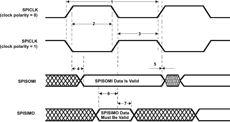 Figure 7-23 SPI Slave Mode External Timing (CLOCK PHASE = 0)
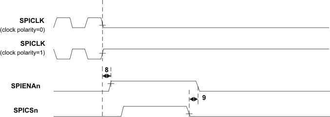 Figure 7-24 SPI Slave Mode Enable Timing (CLOCK PHASE = 0)
Table 7-40 SPI Slave Mode External Timing Parameters (CLOCK PHASE = 1, SPICLK = input, SPISIMO = input, and SPISOMI = output)(1)(2)(3)(4)
| NO. | Parameter | MIN | MAX | Unit | |
|---|---|---|---|---|---|
| 1 | tc(SPC)S | Cycle time, SPICLK(5) | 40 | ns | |
| 2(6) | tw(SPCH)S | Pulse duration, SPICLK high (clock polarity = 0) | 14 | ns | |
| tw(SPCL)S | Pulse duration, SPICLK low (clock polarity = 1) | 14 | |||
| 3(6) | tw(SPCL)S | Pulse duration, SPICLK low (clock polarity = 0) | 14 | ns | |
| tw(SPCH)S | Pulse duration, SPICLK high (clock polarity = 1) | 14 | |||
| 4(6) | td(SOMI-SPCL)S | Dealy time, SPISOMI data valid after SPICLK low (clock polarity = 0) | trf(SOMI) + 20 | ns | |
| td(SOMI-SPCH)S | Delay time, SPISOMI data valid after SPICLK high (clock polarity = 1) | trf(SOMI) + 20 | |||
| 5(6) | th(SPCL-SOMI)S | Hold time, SPISOMI data valid after SPICLK high (clock polarity =0) | 2 | ns | |
| th(SPCH-SOMI)S | Hold time, SPISOMI data valid after SPICLK low (clock polarity =1) | 2 | |||
| 6(6) | tsu(SIMO-SPCH)S | Setup time, SPISIMO before SPICLK high (clock polarity = 0) | 4 | ns | |
| tsu(SIMO-SPCL)S | Setup time, SPISIMO before SPICLK low (clock polarity = 1) | 4 | |||
| 7(6) | tv(SPCH-SIMO)S | High time, SPISIMO data valid after SPICLK high (clock polarity = 0) | 2 | ns | |
| tv(SPCL-SIMO)S | High time, SPISIMO data valid after SPICLK low (clock polarity = 1) | 2 | |||
| 8 | td(SPCH-SENAH)S | Delay time, SPIENAn high after last SPICLK high (clock polarity = 0) | 1.5tc(VCLK) | 2.5tc(VCLK)+tr(ENAn) + 22 | ns |
| td(SPCL-SENAH)S | Delay time, SPIENAn high after last SPICLK low (clock polarity = 1) | 1.5tc(VCLK) | 2.5tc(VCLK)+tr(ENAn) + 22 | ||
| 9 | td(SCSL-SENAL)S | Delay time, SPIENAn low after SPICSn low (if new data has been written to the SPI buffer) | tf(ENAn) | tc(VCLK)+tf(ENAn)+ 27 | ns |
| 10 | td(SCSL-SOMI)S | Delay time, SOMI valid after SPICSn low (if new data has been written to the SPI buffer) | tc(VCLK) | 2tc(VCLK)+trf(SOMI)+ 28 | ns |
For PS values from 1 to 255: tc(SPC)S ≥ (PS +1)tc(VCLK) ≥ 40ns, where PS is the prescale value set in the SPIFMTx.[15:8] register bits.
For PS values of 0: tc(SPC)S = 2tc(VCLK) ≥ 40ns.
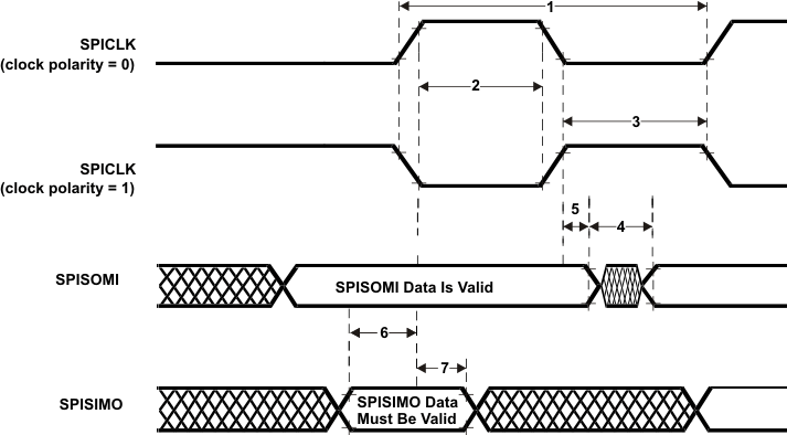 Figure 7-25 SPI Slave Mode External Timing (CLOCK PHASE = 1)
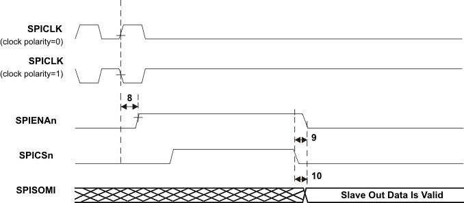 Figure 7-26 SPI Slave Mode Enable Timing (CLOCK PHASE = 1)
7.13 Ethernet Media Access Controller
The Ethernet Media Access Controller (EMAC) provides an efficient interface between the device and the network. The EMAC supports both 10Base-T and 100Base-TX, or 10 Mbits/second (Mbps) and 100 Mbps in either half- or full-duplex mode, with hardware flow control and quality of service (QoS) support.
The EMAC controls the flow of packet data from the device to the PHY. The MDIO module controls PHY configuration and status monitoring.
Both the EMAC and the MDIO modules interface to the device through a custom interface that allows efficient data transmission and reception. This custom interface is referred to as the EMAC control module, and is considered integral to the EMAC/MDIO peripheral. The control module is also used to multiplex and control interrupts.
7.13.1 Ethernet MII Electrical and Timing Specifications
 Figure 7-27 MII Receive Timing
Table 7-41 MII Receive Timing
| Parameter | Description | MIN | MAX |
|---|---|---|---|
| tsu(GMIIMRXD) | Setup time, GMIIMRXD to GMIIMRCLK rising edge | 8ns | |
| tsu(GMIIMRXDV) | Setup time, GMIIMRXDV to GMIIMRCLK rising edge | 8ns | |
| tsu(GMIIMRXER) | Setup time, GMIIMRXER to GMIIMRCLK rising edge | 8ns | |
| th(GMIIMRXD) | Hold time, GMIIMRXD valid after GMIIRCLK rising edge | 8ns | |
| th(GMIIMRXDV) | Hold time, GMIIMRXDV valid after GMIIRCLK rising edge | 8ns | |
| th(GMIIMRXER) | Hold time, GMIIMRXDV valid after GMIIRCLK rising edge | 8ns |
 Figure 7-28 MII Transmit Timing
Table 7-42 MII Transmit Timing
| Parameter | Description | MIN | MAX |
|---|---|---|---|
| td(GMIIMTXD) | Delay time, GMIIMTCLK rising edge to GMIIMTXD | 5ns | 25ns |
| td(GMIIMTXEN) | Delay time, GMIIMTCLK rising edge to GMIIMTXEN | 5ns | 25ns |
7.13.2 Ethernet RMII Timing
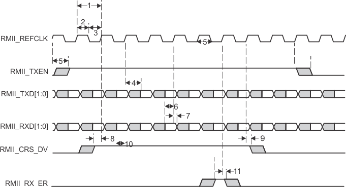 Figure 7-29 RMII Timing Diagram
Table 7-43 RMII Timing Requirements
| NO. | Parameter | Value | Unit | |||
|---|---|---|---|---|---|---|
| MIN | NOM | MAX | ||||
| 1 | tc(REFCLK) | Cycle time, RMII_REF_CLK | - | 20 | - | ns |
| 2 | tw(REFCLKH) | Pulse width, RMII_REF_CLK High | 7 | - | 13 | ns |
| 3 | tw(REFCLKL) | Pulse width, RMII_REF_CLK Low | 7 | - | 13 | ns |
| 6 | tsu(RXD-REFCLK) | Input setup time, RMII_RXD valid before RMII_REF_CLK High | 4 | - | - | ns |
| 7 | th(REFCLK-RXD) | Input hold time, RMII_RXD valid after RMII_REF_CLK High | 2 | - | - | ns |
| 8 | tsu(CRSDV-REFCLK) | Input setup time, RMII_CRSDV valid before RMII_REF_CLK High | 4 | - | - | ns |
| 9 | th(REFCLK-CRSDV) | Input hold time, RMII_CRSDV valid after RMII_REF_CLK High | 2 | - | - | ns |
| 10 | tsu(RXER-REFCLK) | Input setup time, RMII_RXER valid before RMII_REF_CLK High | 4 | - | - | ns |
| 11 | th(REFCLK-RXER) | Input hold time, RMII_RXER valid after RMII_REF_CLK High | 2 | - | - | ns |
| 4 | td(REFCLK-TXD) | Output delay time, RMII_REF_CLK High to RMII_TXD valid | 2 | - | 16 | ns |
| 5 | td(REFCLK-TXEN) | Output delay time, RMII_REF_CLK High to RMII_TX_EN valid | 2 | - | 16 | ns |
7.13.3 Management Data Input/Output (MDIO)
 Figure 7-30 MDIO Input Timing
Table 7-44 MDIO Input Timing Requirements
| NO. | Parameter | Value | Unit | ||
|---|---|---|---|---|---|
| MIN | MAX | ||||
| 1 | tc(MDCLK) | Cycle time, MDCLK | 400 | - | ns |
| 2 | tw(MDCLK) | Pulse duration, MDCLK high/low | 180 | - | ns |
| 3 | tt(MDCLK) | Transition time, MDCLK | - | 5 | ns |
| 4 | tsu(MDIO-MDCLKH) | Setup time, MDIO data input valid before MDCLK High | 12(1) | - | ns |
| 5 | th(MDCLKH-MDIO) | Hold time, MDIO data input valid after MDCLK High | 1 | - | ns |
 Figure 7-31 MDIO Output Timing
Table 7-45 MDIO Output Timing Requirements
| NO. | Parameter | Value | Unit | ||
|---|---|---|---|---|---|
| MIN | MAX | ||||
| 1 | tc(MDCLK) | Cycle time, MDCLK | 400 | - | ns |
| 7 | td(MDCLKL-MDIO) | Delay time, MDCLK low to MDIO data output valid | 0 | 100 | ns |