ZHCSJG7D March   2019  – February 2024 TMUX1101 , TMUX1102

PRODUCTION DATA  

  1.   1
  2. 特性
  3. 应用
  4. 说明
  5. Device Comparison Table
  6. Pin Configuration and Functions
  7. Specifications
    1. 6.1 Absolute Maximum Ratings
    2. 6.2 ESD Ratings
    3. 6.3 Recommended Operating Conditions
    4. 6.4 Thermal Information
    5. 6.5 Electrical Characteristics (VDD = 5V ±10 %)
    6. 6.6 Electrical Characteristics (VDD = 3.3V ±10 %)
    7. 6.7 Electrical Characteristics (VDD = 1.8V ±10 %)
    8. 6.8 Electrical Characteristics (VDD = 1.2V ±10 %)
    9. 6.9 Typical Characteristics
  8. Parameter Measurement Information
    1. 7.1 On-Resistance
    2. 7.2 Off-Leakage Current
    3. 7.3 On-Leakage Current
    4. 7.4 Transition Time
    5. 7.5 Charge Injection
    6. 7.6 Off Isolation
    7. 7.7 Bandwidth
  9. Detailed Description
    1. 8.1 Overview
    2. 8.2 Functional Block Diagram
    3. 8.3 Feature Description
      1. 8.3.1 Bidirectional Operation
      2. 8.3.2 Rail-to-Rail Operation
      3. 8.3.3 1.8V Logic Compatible Inputs
      4. 8.3.4 Fail-Safe Logic
      5. 8.3.5 Ultra-Low Leakage Current
      6. 8.3.6 Ultra-Low Charge Injection
    4. 8.4 Device Functional Modes
      1. 8.4.1 Truth Tables
  10. Application and Implementation
    1. 9.1 Application Information
    2. 9.2 Typical Application - Sample-and-Hold Circuit
      1. 9.2.1 Design Requirements
      2. 9.2.2 Detailed Design Procedure
      3. 9.2.3 Application Curve
    3. 9.3 Typical Application - Switched Gain Amplifier
      1. 9.3.1 Design Requirements
      2. 9.3.2 Detailed Design Procedure
      3. 9.3.3 Application Curve
    4. 9.4 Power Supply Recommendations
    5. 9.5 Layout
      1. 9.5.1 Layout Guidelines
      2. 9.5.2 Layout Example
  11. 10Device and Documentation Support
    1. 10.1 Documentation Support
      1. 10.1.1 Related Documentation
    2. 10.2 接收文档更新通知
    3. 10.3 支持资源
    4. 10.4 Trademarks
    5. 10.5 静电放电警告
    6. 10.6 术语表
  12. 11Revision History
  13. 12Mechanical, Packaging, and Orderable Information

封装选项

请参考 PDF 数据表获取器件具体的封装图。

机械数据 (封装 | 引脚)
  • DBV|5
  • DCK|5
散热焊盘机械数据 (封装 | 引脚)
订购信息

Off Isolation

Off isolation is defined as the ratio of the signal at the drain pin (D) of the device when a signal is applied to the source pin (S) of an off-channel. The characteristic impedance, Z0, for the measurement is 50Ω. Figure 7-6 shows the setup used to measure off isolation. Use off isolation equation to compute off isolation.
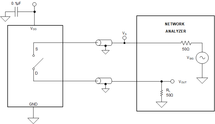
GUID-E975D3DC-4B83-4BD5-B54F-97741D43E5B0-low.gifFigure 7-6 Off Isolation Measurement Setup
Equation 1. GUID-37F7433D-338E-47A4-ADD4-AC4F0163BA41-low.gif