ZHCSJG7D March 2019 – February 2024 TMUX1101 , TMUX1102
PRODUCTION DATA
- 1
- 1 特性
- 2 应用
- 3 说明
- 4 Device Comparison Table
- 5 Pin Configuration and Functions
-
6 Specifications
- 6.1 Absolute Maximum Ratings
- 6.2 ESD Ratings
- 6.3 Recommended Operating Conditions
- 6.4 Thermal Information
- 6.5 Electrical Characteristics (VDD = 5V ±10 %)
- 6.6 Electrical Characteristics (VDD = 3.3V ±10 %)
- 6.7 Electrical Characteristics (VDD = 1.8V ±10 %)
- 6.8 Electrical Characteristics (VDD = 1.2V ±10 %)
- 6.9 Typical Characteristics
- 7 Parameter Measurement Information
- 8 Detailed Description
- 9 Application and Implementation
- 10Device and Documentation Support
- 11Revision History
- 12Mechanical, Packaging, and Orderable Information
封装选项
请参考 PDF 数据表获取器件具体的封装图。
机械数据 (封装 | 引脚)
- DBV|5
- DCK|5
散热焊盘机械数据 (封装 | 引脚)
订购信息
9.3 Typical Application - Switched Gain Amplifier
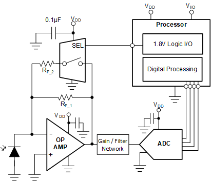
Switches and multiplexers are commonly used in the feedback path of amplifier circuits to provide configurable gain control. By using various resistor values on the switch path, the TMUX110x allows the system to have multiple gain settings. An external resistor ensures the amplifier is not operating in an open loop configuration. A transimpedance amplifier (TIA) for photodiode inputs is a common circuit that requires gain control using a switch to convert the output current of the photodiode into a voltage for the MCU or processor. The amount of light present during a photodiode measurement is dependent on the time of day and available light source. An external switch such as the TMUX110x can be utilized to increase the gain when a smaller photodiode current is present. The leakage current, capacitance, and charge injection performance of the TMUX110x are key specifications to evaluate when selecting a device for gain control. An example switched gain amplifier circuit is shown in Figure 9-4.
 Figure 9-4 Configurable Gain Setting
of a TIA Circuit